
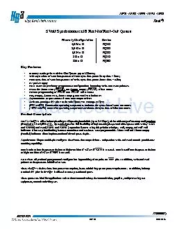
offsets values Parallel programming of PRAF offset values Full Empty Almost Full Almost Empty and Half Full indicators 4096 x 18 FQ245 2048 x 18 FQ235 1024 x 18 FQ225 512 x 18 FQ215 25 ID: 825391
Download Pdf The PPT/PDF document ") and Almost Empty (" is the property of its rightful owner. Permission is granted to download and print the materials on this web site for personal, non-commercial use only, and to display it on your personal computer provided you do not modify the materials and that you retain all copyright notices contained in the materials. By downloading content from our website, you accept the terms of this agreement.


) and Almost Empty () offsets values Pa
) and Almost Empty () offsets values Parallel programming of PRAF offset values Full, Empty, Almost Full, Almost Empty, and Half Full indicators 4,096 x 18 FQ245 2,048 x 18 FQ235 1,024 x 18 FQ225 512 x 18 FQ215 256 x 18 FQ205 pin. In addition, Write and Read pointers to the queue are initialized to zero. These FlexQ I devices have low power consumption, hence minimizing system power requirements. In addition, industry standard 64 - pin Plastic TQFP is offered to save system board space. Page 1 of 26 FQ245 · FQ235 · FQ225 · FQ215 · FQ205 Preliminary Rev 1.05 Volt Synchronous x18 First-In/First-Out QueueKey Features: and ) and Read (REXI and ) expansion features using daisy chain technique. Full, Empty, and Half Full is asserted. Data is read from the queue at the low to high transition of RCLK if REN Page 2 of 26 FQ245 · FQ235 · FQ225 · FQ215 · FQ205 Preliminary Rev 1.0 FQ245FQ235FQ225FQ
215FQ205DATA IN (D17 - 0READ CLOCK (RCL
215FQ205DATA IN (D17 - 0READ CLOCK (RCLK)DATA OUT (Q17 - 0LOAD ( )HALF - FULL FLAG ( )PROGRAMMABLE ( )FULL FLAG ( )WRITE CLOCK (WCLK)WRITE ENABLE ( )PROGRAMMABLE ( )EMPTY FLAG ( )OUTPUT ENABLE ( )READ ENABLE ( )WRITE EXPANSION IN ( )WEXIREAD EXPANSION IN ( )REXIBlock Diagram of Single Synchronous Queue4,096 x 18 / 2 ,048 x 18 / 1,024 x 18 / 512 x 18 / 256 x 18RESET ( )RSTLOADFULLHALFPRAEEMPTYPRAFFIRST LOAD ( )FIRSTWEXOFigure 1. Single Device Configuration Signal Flow Diagram Page 3 of 26 FQ245 · FQ235 · FQ225 · FQ215 · FQ205 Preliminary Rev 1.0 Offset RegisterWrite ControlLogicWrite PointerSRAMInput RegisterOutput RegisterFlag LogicOutputBuffer17-0x1817-0Read PointerRead ControlLogicResetWCLKRCLKRENWENPRAFFULLDRDYEMPTYQRDYExpansion LogicFIRSTWEXIHALFWE
XOREXIREXOHALFWEXORSTFigure 2. Devic
XOREXIREXOHALFWEXORSTFigure 2. Device Architecture Page 4 of 26 FQ245 · FQ235 · FQ225 · FQ215 · FQ205 Preliminary Rev 1.0 178911121314154562PIN 1D10D11GNDQ11VccQ10GNDGNDVccFIRST PRAE Q0REXO FULL REXI PRAF VccWEXIWEN WCLKGND Q3 Q2 GND Q1RCLKLOADGNDEMPTYD17D15RENWEXO/HALFTQFP 64 (Order Code: PF) Top View Figure 3. Device Pin Out Page 5 of 26 FQ245 · FQ235 · FQ225 · FQ215 · FQ205 Preliminary Rev 1.0 Pin # Pin Name Pin Symbol Input/Output Description Input Reset is required to initialize Write and Read pointers to the first position of the queue by setting low. and PRAF will go high; EMPTY and PRAE will go low. All data outputs will go low. Previous programmed configurations will not be maintained. 19 Write Clock WCLK Input Writes data into queue during low to high transitions of WCLK if is set low. 20 Write Enable Input Controls write operation into queue or offset regis
ters during low to high transition of WC
ters during low to high transition of WCLK. Load Enable Input controls write/read, to/from offset registers during low to high transition of WCLK/RCLK respectively. Use in conjunction with WEN/REN18 First Load Input In single device configuration, is set low. In depth expansion configuration, is set low for the first device and set high for other devices in the daisy chain. Write Expansion In Input In single device configuration, is set low. In depth expansion configuration, connected to of previous device in the daisy chain. Data Inputs D17-0 Input 18 - bit wide input data bus. Read Clock RCLK Input Reads data from queue during low to high transitions of RCLK if is set low. 60 Read Enable Input Controls read operation from queue or offset registers during low to high transition of RCLK. Read Expansion In REXI Input In single device configuration, REXI is set low. In depth expansion configura
tion, REXI is connected of previous de
tion, REXI is connected of previous device in the daisy chain. 58 Output Enable Input Setting low activates the data output drivers. Setting high deactivates the data output drivers (High-Z). Data Outputs Q17-0 Output 18 - bit wide output data bus. Read Expansion Out Output In depth expansion configuration,connected to REXI of next device in the daisy chain. 25 Full Flag Output Queue is full when goes low during the low to high transition of WCLK. This prohibits further writes into the queue. Table 1. Pin Descriptions Page 6 of 26 FQ245 · FQ235 · FQ225 · FQ215 · FQ205 Preliminary Rev 1.0 Pin # Pin Name Pin Symbol Input/Output Description 54 Empty Flag EMPTY Output Queue is empty when EMPTY goes low during the low to high transition of RCLK. This prohibits further reads from the queue. 23 Almost Full PRAF Output Queue is almost full when PRAF goes low during the low to high transiti
on of WCLK. Default (Full-offset) or pr
on of WCLK. Default (Full-offset) or programmed offset values determine the status of PRAF. 17 Almost Empty PRAE Output Queue is almost empty when goes low during the low to high transition of RCLK. Default (Empty+offset) or programmed offset values determine the status of PRAE. Write Expansion Out/Half Full WEXO/HALF Output In single device configuration, queue is more than half full when WEXO/HALF goes low. In depth expansion configuration, WEXO/connected to of next device in the daisy chain. 22, 33, 43, 49, 56 Power Vcc N/A 5V power supply. Ground GND N/A 0V Ground. Table 1. Pin Descriptions (Continued) Page 7 of 26 FQ245 · FQ235 · FQ225 · FQ215 · FQ205 Preliminary Rev 1.0 Symbol Rating Coml & Indl Unit TERMTerminal Voltage with respect to GND -0.5 to + 7 V Storage Temperature -55 to +125 DC Output Current -50 to +50 mA NOTES: Absolute Max Ratings are for reference only. Permanen
t damage to the device may occur if exte
t damage to the device may occur if extended period of operation is outside this range. Standard operation should fall within the Recommended Operating ConditionsTable 2. Absolute Maximum Ratings FQ245 FQ235 FQ225 FQ215 FQ205Commercial Clock = 7.5ns, 10ns, 15ns Industrial Clock = 10ns, 15ns Symbol Parameter Min. Typ. Max. Min. Typ. Max. Unit Recommended Operating Conditions Supply Voltage Coml/Indl 4.5 5.0 5.5 4.5 5.0 5.5 V GND Supply Voltage 0 0 0 0 0 0 V Input High Voltage Coml/Indl 2.0 - 5.0 2.0 - 5.0 V Input Low Voltage Coml/Indl - - 0.8 - - 0.8 V Operating Temperature Commercial 0 - 70 0 - 70 Operating Temperature Industrial -40 - 85 -40 - 85 DC Electrical Characteristics (1)Input Leakage Current (any input) -10 - 10 -10 - 10 Output Leakage Current -10 - 10 -10 - 10 Output Logic 1 Voltage, IOH=-2mA 2.4 - - 2.4 - - V Output Logic 0 Voltage, IOL = 8mA - - 0.4 - - 0.4 V Power Cons
umption (2,3)Active Power Supply Curr
umption (2,3)Active Power Supply Current - - 20 - - 20 mA (4)Standby Current - - 5 - - 5 mA Table 3. DC Specifications Page 8 of 26 FQ245 · FQ235 · FQ225 · FQ215 · FQ205 Preliminary Rev 1.0 Capacitance at 100MHz Ambient Temperature (25°C) Symbol Parameter Conditions Max. UnitInput Capacitance VIN= 0V 10 pF (2,4)Output Capacitance VOUT= 0V 10 pF NOTES: 1. Measurement with 0.4N2. With output tri-stated (OE = High) 3. Icc(1,2) is measured with WCLK and RCLK at 20 MHz 4. Design simulated, not tested. Table 3. DC Specifications (Continued) Page 9 of 26 FQ245 · FQ235 · FQ225 · FQ215 · FQ205 Preliminary Rev 1.0 Commercial Commercial & Industrial FQ245-7.5 FQ235-7.5 FQ225-7.5 FQ215-7.5 FQ205-7.5 FQ245-10 FQ235-10 FQ225-10 FQ215-10 FQ205-10 FQ245-15 FQ235-15 FQ225-15 FQ215-15 FQ205-15 Symbol Parameter Min. Max. Min. Max. Min. Max. Unit fs Clock Cycle Frequency - 133 - 100 - 66.7 MHz Data
Access Time 1 5 2 6.5 2 10 ns WCLK Writ
Access Time 1 5 2 6.5 2 10 ns WCLK Write Clock Cycle Time 7.5 - 10 - 15 - ns WCLKH Write Clock High Time 3.5 - 4.5 - 6 - ns WCLKL Write Clock Low Time 3.5 - 4.5 - 6 - ns RCLK Read Clock Cycle Time 7.5 - 10 - 15 - ns RCLKH Read Clock High Time 3.5 - 4.5 - 6 - ns RCLKL Read Clock Low Time 3.5 - 4.5 - 6 - ns Data Set-up Time 2.5 - 3 - 4 - ns Data Hold Time 0.5 - 0.5 - 1 - ns ENS Enable Set-up Time 2.5 - 3 - 4 - ns ENH Enable Hold Time 0.5 - 0.5 - 1 - ns Reset Pulse Width(1) 10 - 10 - 15 - ns RSS Reset Set-up Time 10 15 - 10 - ns RSR Reset Recovery Time 10 - 15 - 10 - ns RSF Reset to Flag and Output Time - 12 - 15 - 20 ns OLZ Output Enable to Output in Low-Z(2) 0 - 0 - 0 - ns Output Enable to Output Valid 2 5 3 6 3 8 ns OHZ Output Enable to Output in High-Z(2) 2 5 3 6 3 8 ns FULL Write Clock to Full Flag - 5 - 6.5 - 10 ns EMPTY Read Clock to Empty Flag - 5 - 6.5 - 10 ns PRAF Clock to Programmable Al
most-Full Flag - 13 - 17 - 24 ns PRAE C
most-Full Flag - 13 - 17 - 24 ns PRAE Clock to Programmable Almost-Empty Flag - 13 - 17 - 24 ns HALF Clock to Half-Full Flag - 13 - 17 - 24 ns Clock to Expansion Out - 5 - 6.5 - 10 ns Expansion in Pulse Width 3 - 3 - 6.5 - ns XIS Expansion in Set-Up Time 3.5 - .5 - 5 - ns SKEW1Skew time between Read Clock & Write Clock for Full Flag 4 - 5 - 6 - ns SKEW2Skew time between Read Clock & Write Clock for Empty Flag 4 - 5 - 6 - ns NOTES: 1. Pulse widths less than minimum values are not allowed. 2. Design simulated, not tested. Table 4. AC Electrical Characteristics Page 10 of 26 FQ245 · FQ235 · FQ225 · FQ215 · FQ205 Preliminary Rev 1.0Input Pulse Levels GND to 3.0V Input Rise/Fall Times 3ns Input Timing Reference Levels 1.5V Output Reference Levels 1.5V Output Load*, clock = 10ns, 15ns See Figure 5 Output Load, clock = 6ns, 7.5ns See Figure 4 *Include jig and scope capacitances Table 5. AC Test Condition
D.U.T.68030pF*1.1kFigure 5. Output Load*
D.U.T.68030pF*1.1kFigure 5. Output Load*Includes jig and scope capacitances.for clock = 10ns, 15nsVcc/2Z0 = 50Figure 4. AC Test Loadfor clock = 7.5ns Page 11 of 26 FQ245 · FQ235 · FQ225 · FQ215 · FQ205 Preliminary Rev 1.0Pin Functions Reset is required to initialize Write and Read pointers to the first position of the queue by setting low. and will go high; EMPTYand will go low. All data outputs will go low. Previous programmed configurations will not be maintained.WCLK Writes data into queue during low to high transitions of WCLK if is set low. Synchronizes and flags. WCLK and RCLK are independent of each other.Controls write operation into queue or offset registers during low to high transition of WCLK.LOADcontrols write/read, to/from offset registers during low to high transition of WCLK/RCLK respectively for parallel programming. Use in conjunction with WEN/RENIn single device configurati
on, is set low. In depth expansion con
on, is set low. In depth expansion configuration, is set low for the first device and set high for other devices in the daisy chain. In single device configuration, is set low. In depth expansion configuration, is connected to of previous device in the daisy chain. 17-018 - bit wide input data bus.RCLK Reads data from queue during low to high transitions of RCLK if is set low. Synchronizes the EMPTYand flags. RCLK and WCLK are independent of each other.Reads data from queue during low to high transitions of RCLK if is set to low. This also advances the Read pointer of the queue.Setting low activates the data output drivers. Setting high deactivates the data output drivers (High-Z). does not control advancement of Read pointer.17-0 18 - bit wide output data bus.In depth expansion configuration, is connected to REXIof next device in the daisy chain. Queue is full when goes low during the low t
o high transition of WCLK. This prohibi
o high transition of WCLK. This prohibits further writes into the queue and prevents advancement of Write pointer. Refer to Table 8 for behavior of FULL. Queue is empty when EMPTYgoes low during the low to high transition of RCLK. This prohibits further reads from the queue and prevents advancement of Read pointer. Refer to Table 8 for behavior of EMPTY.Queue is almost full when goes low during the low to high transition of WCLK. PRAF goes high during the low to high transition of RCLK. Default (Full-offset) or programmed offset values determine the status of PRAF. Refer to Table 8 for behavior of PRAF.Queue is almost empty when PRAE goes low during the low to high transition of RCLK. goes high during the low to high transition of WCLK. Default (Empty+offset) or programmed offset values determine the status of PRAE. Refer to Table 8 for behavior of PRAE.WEXO/HALF In single device configurati
on, queue is more than half full when g
on, queue is more than half full when goes low during the low to high transition of WCLK. Queue is less than half full when HALF goes high during the low to high transition of RCLK. Refer to Table 8 for details. In depth expansion configuration, is connected to of next device in the daisy chain In single device configuration, REXI is set low. In depth expansion configuration, REXI is connected to of previous device in the daisy chain. Page 12 of 26 FQ245 · FQ235 · FQ225 · FQ215 · FQ205 Preliminary Rev 1.0 WCLK FQ245 FQ235 FQ225 FQ215 FQ205 Selection / Sequence 0 0 1 Parallel write to offset Empty Offset Full Offset Parallel write to 0 1 0 X Parallel read from offset Empty Offset Full Offset Parallel read from registers: X 1 1 X X No Operation 1 0 X X Write Memory 1 X 0 X Read Memory 1 1 1 X X No Operation Figure 6. Programmable Flag Offset Programming Sequence PRAFP
rogramming (bits)PRAEProgramming (bits)
rogramming (bits)PRAEProgramming (bits)FQ245 D/Q11-0 D/Q11-0 FQ235 D/Q10-0 D/Q10-0 FQ225 D/Q9-0 D/Q9-0 FQ215 D/Q8-0 D/Q8-0 FQ205 D/Q7-0 D/Q7-0 Table 6. Parallel Offset Register Data Mapping Table Default FQ245 007FH FQ235 007FH FQ225 007FH FQ215 003FH FQ205 001FH Table 7. Default Values of Offset Registers Page 13 of 26 FQ245 · FQ235 · FQ225 · FQ215 · FQ205 Preliminary Rev 1.0 # of Bits for Offset Registers 12 bits for FQ245 11 bits for FQ235 10 bits for FQ225 9 bits for FQ215 8 bits for FQ205 Note: Dont Care applies to all unused bits Figure 7. Parallel Offset Write/Read Cycles Diagram Data WidthData WidthData WidthData WidthFQ245 4,096 x 18FQ235 2,048 x 18FQ225 1,024 x 18FQ215 512 x 1839119119899D/Q8D/Q6D/Q4D/Q2D/Q0D/Q7D/Q5D/Q3D/Q1D/Q9D/Q10D/Q11D/Q12D/Q13D/Q14D/Q15D/Q16D/Q17D/Q
8D/Q6D/Q4D/Q2D/Q0D/Q7D/Q5D/Q3D/Q
8D/Q6D/Q4D/Q2D/Q0D/Q7D/Q5D/Q3D/Q1D/Q9D/Q10D/Q11D/Q12D/Q13D/Q14D/Q15D/Q16D/Q17D/Q8D/Q6D/Q4D/Q2D/Q0D/Q7D/Q5D/Q3D/Q1D/Q9D/Q10D/Q11D/Q12D/Q13D/Q14D/Q15D/Q16D/Q17D/Q8D/Q6D/Q4D/Q2D/Q0D/Q7D/Q5D/Q3D/Q1D/Q9D/Q10D/Q11D/Q12D/Q13D/Q14D/Q15D/Q16D/Q17PRAEPRAF1st Cycle2nd CyclePRAEPRAF1st Cycle2nd CyclePRAEPRAF1st Cycle2nd CycleData WidthFQ205 256 x 184D/Q8D/Q6D/Q4D/Q2D/Q0D/Q7D/Q5D/Q3D/Q1D/Q9D/Q10D/Q11D/Q12D/Q13D/Q14D/Q15D/Q16D/Q17PRAEPRAF1st Cycle2nd CyclePRAEPRAF1st Cycle2nd Cycle Page 14 of 26 FQ245 · FQ235 · FQ225 · FQ215 · FQ205 Preliminary Rev 1.0 FQ245 PRAF HALF PRAE EMPTY 0 H H H L L (1) H H H L H (y+1) to 2,048 H H H H H 2,049 to [4,096-(x+1)] H H L H H (4,096 -x(2)) to 4,095 H L L H H 4,096 L L L H H FQ235 PRAF HALF PRAE EMPTY 0 H H H L L (1) H H H L H (y+1) to 1,024 H H H H H 1,025 to [2,048-(x+1)] H H L H H (2,048 -x(2)) to 2,047 H L
L H H 2,048 L L L H H FQ225 PRAF
L H H 2,048 L L L H H FQ225 PRAF HALF PRAE EMPTY 0 H H H L L (1) H H H L H (y+1) to 512 H H H H H 513 to [1,024-(x+1)] H H L H H (1,024 x(2)) to 1,023 H L L H H 1,024 L L L H H FQ215 PRAF HALF PRAE EMPTY 0 H H H L L (1) H H H L H (y+1) to 256 H H H H H 257 to [512-(x+1)] H H L H H (512 -x(2)) to 511 H L L H H 512 L L L H H FQ205 PRAF HALF PRAE EMPTY 0 H H H L L (1) H H H L H (y+1) to 128 H H H H H 129 to [256-(x+1)] H H L H H (256 x(2)) to 255 H L L H H 256 L L L H H NOTES: 1. y = PRAEoffset. Default Values: FQ205 y = 31, FQ215 y = 63, FQ245/FQ235/FQ225 y = 127. 2. x = PRAFoffset. Default Values: FQ205 y = 31, FQ215 y = 63, FQ245/FQ235/FQ225 y = 127.Table 8. Status Flags Page 15 of 26 FQ245 · FQ235 · FQ225 · FQ215 · FQ205 Preliminary Rev 1.0Timing Diagrams NOTES: 1. After reset, the outputs will be low if OE = 0 and tri-state if OE=1. 2. The clocks (RCLK, WCL
K) can be free-running during reset. Dia
K) can be free-running during reset. Diagram 1. Reset Timing RSRRSFRSFRSF = 1 = 017 - 0RSTLOADWENRENPRAEEMPTYHALFPRAFFULLOE Page 16 of 26 FQ245 · FQ235 · FQ225 · FQ215 · FQ205 Preliminary Rev 1.0 WCLKENSFULLSKEW1Data ValidNo OperationWCLK17 - 0RCLKWENRENWCLKLWCLKHFULLNOTES: 1. tSKEW1 is the minimum time between a rising RCLK edge and rising WCLK edge to guarantee that FULLwill go high during the current clock cycle. If the time between the rising edge of RCLK and the rising edge of WCLK is equal to or less than tSKEW1, then FULLmay not change state until the next WCLK edge. Diagram 2. Write Cycle Timing Page 17 of 26 FQ245 · FQ235 · FQ225 · FQ215 · FQ205 Preliminary Rev 1.0 RCLKRCLKLRCLKHEMPTYSKEW2OHZEMPTYValid DataOLZENSENH17 - 0RCLKRENEMPTYWCLKWENNOTES1. tSKEW1 is the minimum time between a rising W
CLK edge and a rising RCLK edge to guara
CLK edge and a rising RCLK edge to guarantee that EMPTY will go high during the current clock cycle. If the time between the rising edge of WCLK and the rising edge of RCLK is less than tSKEW1, then EMPTY may not change state until the next RCLK edge.Diagram 3. Read Cycle Timing Page 18 of 26 FQ245 · FQ235 · FQ225 · FQ215 · FQ205 Preliminary Rev 1.0 ENSFRL(1)OLZENSEMPTYSKEW2WCLK17 - 017 - 0WENEMPTYNOTES: 1. tFRL is the latency from first write to first Read. When tSKEW2 is greater than or equal to minimum specification, tFRL (maximum) = tRCLK + tSKEW2. When tSKEW2 is less than minimum specification, tFRL (maximum) equals either 2* tRCLK + tSKEW2 or tRCLK + tSKEW2. The Latency Timing applies only at the Empty Boundary (EMPTY= low).Diagram 4. First Data Word Latency after Reset with Simultaneous Read and Write Page 19 of 26 FQ245 · FQ235 · F
Q225 · FQ215 · FQ205 Preliminary Rev 1.
Q225 · FQ215 · FQ205 Preliminary Rev 1.0 Output Register DataData ReadNext Data ReadLOWData WriteData WriteNo WriteNo WriteSKEW 1(1)FULLFULLFULLENSENHENHAtAWCLK17 - 017 - 0SKEW 1(1)RENWENFULLNOTES: 1. tSKEW1 is the minimum time between a rising RCLK edge and a rising WCLK edge to guarantee that FULLwill go high during the current clock cycle. If the time between the rising edge of RCLK and the rising edge of WCLK is le than tSKEW1, then FULL may not change state until the next WCLK edge. Diagram 5. Full Flag Timing Page 20 of 26 FQ245 · FQ235 · FQ225 · FQ215 · FQ205 Preliminary Rev 1.0 Output Register Data DWFRL(1)SKEW2SKEW2FRL(1)EMPTYENHENSENSENHWCLK17 - 0RCLK17 - 0LOWEMPTYWENEMPTYEMPTYRENNOTES: 1. tFRL is the latency from first write to first Read. When tSKEW2 is greater than or equal to minimum specification, tFRL (maximum) = tRCLK + t SKEW2
When tSKEW2 less than minimum speci
When tSKEW2 less than minimum specification, tFRL (maximum) equals either 2 * tRCLK + tSKEW2, or tRCLK + tSKEW2. The Latency Timing applies only at the Empty Boundary (EMPTY= low). Diagram 6. Empty Flag Timing Page 21 of 26 FQ245 · FQ235 · FQ225 · FQ215 · FQ205 Preliminary Rev 1.0 WCLKLWCLKHWCLKENSoffsetoffsetoffset11 - 0WCLKoffsetWENLOADPRAEPRAEPRAFPRAFDiagram 7. Write Programmable RegistersRCLKLRCLKHRCLKENHENSENSRCLKAoffsetoffsetLOADRENPRAEPRAFoffsetPRAEoffsetPRAFDiagram 8. Read Programmable RegistersWCLKLWCLKHy + 1 words in Queuey words in QueueWCLKRCLKENHy words in QueueWENPRAERENNOTES:1. y = PRAEoffset. Diagram 9. Programmable Almost-Empty Flag Timing Page 22 of 26 FQ245 · FQ235 · FQ225 · FQ215 · FQ205 Preliminary Rev 1.0 WCLKLWCLKHD - x words in QueuememoryD - (x+1) words in Queuememory(1)WCLKD - (x+1) words in Queue memoryWENPRAFNOT
ES:1. x = PRAFoffset. 2. D = maximum
ES:1. x = PRAFoffset. 2. D = maximum queue depth = 256 words for FQ205; 512 words for FQ215; 1,024 words for FQ225; 2,048 words for FQ235; and 4,096 words for FQ1V245. Diagram 10. Programmable Almost-Full Flag TimingWCLKLWCLKHHALFD/2 + 1 words inQueue memory(2)D/2 words in QueuememoryWCLKRCLKENSD/2 words in Queue memoryWENHALFRENNOTES:1. D = maximum queue depth = 256 words for FQ205; 512 words for FQ215; 1,024 words for FQ225; 2,048 words for FQ235; and 4,096 words for FQ1V245. Diagram 11. Half-Full Flag Timing Page 23 of 26 FQ245 · FQ235 · FQ225 · FQ215 · FQ205 Preliminary Rev 1.0 WCLKWENWEXONote 1NOTES: 1. Write to Last Physical Location.Diagram 12. Write Expansion Out Timing RCLKNote 1tREXORENNOTES: 1. Read from Last Physical Location. Diagram 13. Read Expansion Out Timing WCLKWEXIDiagram 14. Write Expansion in Timing RCLKXISREXIDiagram 15. Read Expansion in Timing Page 24 of 26
FQ245 · FQ235 · FQ225 · FQ215 · FQ205 Pr
FQ245 · FQ235 · FQ225 · FQ215 · FQ205 Preliminary Rev 1.0Width Expansion Configuration Simply connecting together the control signals of multiple devices may increase word width. Status flags can be detected from any one device. The exceptions are the Empty Flag and Full Flag. Because of variations in skew between RCLK and WCLK, it is possible for flag assertion and de-assertion to vary by one cycle between FIFOs. To avoid problems the user must create composite flags by ANDing the Empty Flags of every FIFO, and separately ANDing all Full Flags. Figure 7 demonstrates a 36-bit width by using two FQ245 / 235 / 225 / 215 / 205s. Any word width can be attained by adding additional FQ245 / 235 / 225 / 215 / 205s. RESET ( )DATA IN (D)WRITE CLOCK (WCLK)LOAD ( )PROGRAMMABLE ( )HALF- FULL ( )RESET ( )36181836DATA OUT (Q)READ CLOCK (RCLK)FULL ( )PROGRAMMABLE (
)FIRST LOAD ( )WRITE EXPA
)FIRST LOAD ( )WRITE EXPANSION IN ( )READ EXPANSION IN ( )Block Diagram of Synchronous Queue4,096 x 36 / 2,048 x 36 / 1,024 x 36 / 512 x 36 / 256 x 36RSTRSTOUTPUT ENABLE ( )READ ENABLE ( )PRAFEMPTY FLAG ( )EMPTYFIRSTWEXIREXIEMPTYEMPTYFULLFULLFULLHALFWRITE ENABLE ( )WENLOADPRAENOTES:1. Do not connect any output control signals directly together. Figure 7. Width Expansion Configuration Page 25 of 26 FQ245 · FQ235 · FQ225 · FQ215 · FQ205 Preliminary Rev 1.0Depth Expansion Configuration (with Programmable Flags) These devices can easily be adapted to applications requiring more than 4,096 / 2,048 / 1,024 / 512 / 256 words of buffering. Figure 8 shows Depth Expansion using three FQ245 / 235 / 225 / 215 / 205s. Maximum depth is limited only by signal loading. Follow these steps: The first device must be designated by grounding t
he First Load () control input. All o
he First Load () control input. All other devices must havein the high state. The Write Expansion Out () pin of each device must be tied to the Write Expansion In () pin of the next device. The Read Expansion Out () pin of each device must be tied to the Read Expansion In () pin of the next device. All Load () pins are tied together. The Half-Full Flag () is not available in this Depth Expansion Configuration. , and are created with composite flags by ORing together every respective flags for monitoring. The composite and flags are not precise. DATA OUTREAD CLOCKREAD ENABLELOADRESETWRITE ENABLEWRITE CLOCKDATA INVccVccFIRST LOAD ( )OUTPUT ENABLEBlock Diagram of Synchronous Queue12,288 x 18 / 6,144 x 18 / 3,072 x 18 / 1,536 x 18 / 768 x 18WEXIREXIFIRSTPRAFFULLPRAEEMPTYWCLKFQV245FQV235FQV225FQV215FQV205WEXOREXOWENRENRSTLOADFULLPRAFWEXIREXIPRAEEMPTYRCLKFQV245FQV23
5FQV225FQV215FQV205WEXOREXORENRSTLO
5FQV225FQV215FQV205WEXOREXORENRSTLOADFULLPRAFPRAEEMPTYFIRSTWEXIREXIRCLKFQV245FQV235FQV225FQV215FQV205WEXOWENRSTLOADFULLPRAFPRAEEMPTYFIRSTFigure 8. Block Diagram of Multiple Devices with Programmable Flags used in Depth Expansion Configuration Page 26 of 26 FQ245 · FQ235 · FQ225 · FQ215 · FQ205 Preliminary Rev 1.0Order Information: Speed 7.5ns available only in Commercial (0°C to 70°C) *Package 64 pin Plastic Thin Quad Flat Pack (TQFP) Example: FQ235L7-5PF (32k x 18, 7.5ns, Commercial temp) FQ225L10PFI (16k x 18, 10ns, Industrial temp) High Bandwidth Access 2107 North First Street, Suite 415 San Jose, CA 95131, USA HBA Device Family Device Type Power Speed (ns)* Package** Temperature Range XX XXX X XX XX XFQ 245 (4,096 x 18) ow 7-5 133 MHz Blank Commercial (0°C to 70°C) (2,048 x 18 100 MHz Industrial (-40° to 85°C) (1,024 x 18) 66 MHz (512 x 18) (256 x