
1Introduction 1Introduction2SiGeMarket Survey 2SiGeMarket Survey3Fundamentals of SiGe CVD 3Fundamentals of SiGe CVD4CVD Equipment for SiGe 4CVD Equipment for SiGe5Device aplications and 5De ID: 824937
Download Pdf The PPT/PDF document "SiGe CVD,fundamentals and device applica..." is the property of its rightful owner. Permission is granted to download and print the materials on this web site for personal, non-commercial use only, and to display it on your personal computer provided you do not modify the materials and that you retain all copyright notices contained in the materials. By downloading content from our website, you accept the terms of this agreement.


SiGe CVD,fundamentals and device applica
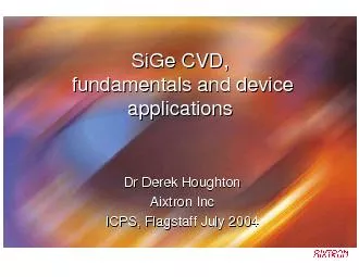
SiGe CVD,fundamentals and device applicationsSiGe CVD,fundamentals and device applicationsDr Derek HoughtonAixtron IncICPS, Flagstaff July 2004Dr Derek HoughtonAixtron IncICPS, Flagstaff July 20041.Introduction1.Introduction2.SiGeMarket Survey2.SiGeMarket Survey3.Fundamentals of SiGe CVD3.Fundamentals of SiGe CVD4.CVD Equipment for SiGe4.CVD Equipment for SiGe5.Device aplications and 5.Device aplications and 6.SiGe materials engineering, metrology6.SiGe materials engineering, metrology7.Summaryand Discussion7.Summaryand DiscussionSiGesMarket Opportunity...SiCMOS/BJTsSiGe HBTs/CMOS?III-V FETs/HBTsRoadNavigation/AreospaceFrequency (GHz)SiGeHBT device structure and process descriptionOnlydifference: BaseSiGe replacesSiliconKeyfiguresofSiGeHBTprocessKeyfiguresofSiGeHBTprocessSiGe BiCMOSuses SiGeHBT + SiSiGeHBT shows same process as SiBT with exception of 30-80 nm thin SiGebase layer (Ge25%)Growth rates used are about 30 Typically, same LPCVD growth chambers can depositeboth Siand SiGelayersDepending on SiGeHBT process, SiGe BiCMOSuses SiGeHBT + SiSiGeHBT shows same process as SiBT with exception of 30-80 nm thin SiGebase layer (Ge25%)Growth rates used are about 30 Typically, same LPCVD growth chambers can depositeboth Siand SiGelayersDepending on SiGeHBT process, SiGeIC forecast by market, 2000 to 2005, in mil. US$2004006008001000120014001600180020032004CAGR=+125%CAGR=+125%SiGeIC Market [Mio. US$]SiGeviable alternative to GaAsMain markets being targeted:Cellular / Cordless / WLANFO-DatacomPC interface cards / LANFuture trends:integrated low power RF-First choice for up/down will dominate 40 GbpsSiGeviable alternative to GaAsMain markets being targeted:Cellular / Cordless / WLANFO-DatacomPC interface cards / LANFuture trends:integrated low power RF-First choice for up/down will dominate 40 GbpsSource: Strategies Unlimited, 1999CAGR: CompoundAverageGrowth RateStrained Si: prototypes from Intel, IBM & UMC demonstratedAlmost all large Si-CMOS manufacturers are presenting cross sectional pictures of CMOS transistors (with gate lengths between 65 and 90 nm) which use Strained-Si technology. Intel and IBM use their own technology, whereas UMC is Amberwavestechnology:process and actual statusStrained Si technology enables improvement in CMOS performance and functionality via replacement of the bulk, cubic-crystal Si Different types of processes developed and patented by the main players: Amberwave(IQE) -AIXTRON, IBM,Toshiba & IntelFirst demos of perfect working 52 Mbit SRAMswith 90 nm CMOS devices on 300 Pentium 4 production with Str.-Siplanned for Process and substrate costs still not 100% fixed. Price expectations for substrate from Strained Si technology enables improvement in CMOS performance and functionality via replacement of the bulk, cubic-crystal Si Different types of processes developed and patented by the main players: Amberwave(IQE) -AIXTRON, IBM,Toshiba & IntelFirst demos of perfect working 52 Mbit SRAMswith 90 nm CMOS devices on 300 Pentium 4 production with Str.-Siplanned for Process and substrate costs still not 100% fixed. Price expectations for substrate from Actual status Strained-SiprocessActual status Strained-SiprocessStrained Si process of Amberwave: One of the Strained Si pioneersTypically, 2 to 4 µm thick graded SiGebuffer layer, followed by thin ()channel layerDepending on substrate Geconcentration, clear mobility and Through Amberwaves proprietary chemical-mechanical polishing (CMP) intermediate process, SiGe buffer layer Typically, 2 to 4 µm thick graded SiGebuffer layer, followed by thin ()channel layerDepending on substrate Geconcentration, clear mobility and Through Amberwaves proprietary chemical-mechanical polishing (CMP) intermediate process, SiGe buffer layer StrainedSilicon CMOS technology Strained silicon mainly addresses high-end digital CMOS markets20000400006000080000100000200004000060000800001000002003200420052006CAGR*= 12.5%CAGR*= 12.5%Digital CMOS Electronic Market [Mio. US$]Si FPGAsSiDigital Signal Processors (DSPs)SiMicroprocessors (MPUs)SiMicro-controllers (MCUs)Digital electronic market forecast and expected strained Sipenetration, 2003 to 2007, in mil. US$Source:VLSI Research, 2002�CAGR*= 200%�CAGR*= 200%Strained Sibased CMOS Market [Mio. US$]20032004200520062007Source:AIXTRON estimatesAssumptionsAssumptionsMain application will be high-end Main markets being targeted: PCs, workstations, game Future trends: Strained Si Main application will be high-end Main markets being targeted: PCs, workstations, game Future trends: Strained Si CAGR:CompoundAverageGrowth RateCarbon and Oxygen concentrations (cmRCA + 4 hours in air + HF dipRCA + HF dip0500100015002000250030003500Partial pressure for oxygen incorporation from H2O and O2AIX 2600G3: up to 7x150 or3x200 mmTricentSiGeCluster Tool: 150, 200 or300 AIXTRONs flexible episystems for StrainedSi / SiGe SiGeUHVCVDSiHB2H6P~ 10-3ghydrogen terminated Siwafers at startHot wall UHVCVD Batch toolUniform Gas Distribution byAIXTRON´s Closed Coupled ShowerheadGrowth RateDistance to gas inletClosed Coupled Showerhead ReactorHorizontal Quarz Tube ReactorGrowth RateDistance to gasinletSiGe Tricent®Water-CooledReactorLidShowerhead Detail Temperature Control ConceptProcessSubstrCoatedGraphiteSiGe TricentUnique CVD chamber featuresTemperature controlTemperature controlCustomer ProcessSupportCleanRoom WallCassette TempProcessGas Sources550-680°CSiGe:CSiH4 + GeH4 + SiCH6650-750°CSiGeSiH4 + GeH4730-800°Csel. SiGeSiH2Cl2 + HCl+ GeH4800-900°CSEGSiH2Cl2 + HClHBTs, HFETsand BiCMOS-pure Silicon Growth-differential SiGe:C growth -selective SiGe:C growth-SiGe on SOI SiGeHBT in a BiCMOSflowLOCOS+PolysiliconEmitterSpacersEpitaxialLayer N+XTEM of Si deposition on Si/oxideHBT base structure SIMS profiling050010001500Germanium conc. (%)SIMS analysis (cameca)GeGummelPlot, npnHBT00.20.40.60.811.21.4(A)NPN11A, CVD-140Triangular SiGebase profile= 0.6 x 1.2 micronCMOS transistorSelective SiGeEpitaxyDC Houghton J.Appl.Phys.1991Strained Silicon on SOI wafer by layer transferStrained Silicon on graded SiGe bufferAmberwaveStrained SiStrained SiSiGe stackSiGe gradeSi substrateSi substrateDCD x ray diffractionSIMS profileStrainedSi Graded SiGeBufferCsCascade ScientificCounts Per Second12C16OSample A312/04/2003024810Strained Si layersSiGe graded 5...40%SiGe 40%Low defect density Gewithout SiGe graded bufferGeSi waferCross sectional TEMPlan view TEM(looking down through Ge cap)Growth Rate vs Germanium concentration0510152025303540Rate @ 495°Rate @ 525°Geconcentration (%)Growth Rates vsTemperature1.11.151.21.251.31.35Reactant LimitedGrowth rate (nm/minute)SiGe/SiMultilayer structureAbrupt Si/SiGeinterfaces SiGeMulti Quantum Wells (MQW)SIMS010002000300040005000Concentration (Ge%)Sample ACsCascade ScientificSIMSCounts Per SecondXRD10010110210310410-3000-2000-10000100020003000Intensity (cps)th\2th (sec)Reference (Active)Double crystal X-ray data Periodof super-lattice = 39.5nmMean Gefraction of structure (Sispacers + SiGeWells) = 0.6%Measured by SiGeMulti Quantum Wells (MQW)Raman ScatteringRaman ScatteringFourier transform low temperature photoluminescence apparatus.CryostatSAMPLEMovingMirrorBeam-splitterGermaniumDetectorExcitation SourceFourierSpectrometerLaser90010001100Photoluminescence IntensityVerticalProfileSiGePatternedWaferSiGeLayerSi SurroundSiGeEtched OffEnergy - meVPL spectra from SiGeHBT transistors1E-30.010.1SiGe PL Threshold & Saturation EffectsSample BAs GrownSample BAnnealedSample AAs GrownSiGe PL Peak Height Incident Photon Flux / s9801000102010401060100PL IntensityEnergy / meVPL SpectraSample B Annealed1.4x103.5x10SiGe - Graded Composition15%CarrierWavefunctionGe Profile 20 nm SiPL of SiGeHBTPhotoluminescenceMappingofCompositionandBandgapona6"waferSamplepoint"NP"energy(meV)Energybandgap(meV)Composition(%ofGe)a10801092.28.97b1082.51094.78.69c1085.21097.48.39d1083.31095.58.60e1082.51094.78.69f1084.81097.08.44g1083.71095.98.56h10791091.29.08abdcefgAuger Electron Spectroscopy Of Graded germanium concentration profiles020004000600080001 10Actual profileGermanium atomic concentration (%)Sputtering time (s)HBT profileFET profilePure Ge, III-Vs on Ge on SiGe, epitaxial metals1E-30.010.1SiGe PL Threshold & Saturation EffectsSample BAs GrownSample BAnnealedSample AAs GrownSiGe PL Peak Height Incident Photon Flux / s9801000102010401060100PL IntensityEnergy / meVPL SpectraSample B Annealed1.4x103.5x10SiGe - Graded Composition15%CarrierWavefunctionGe Profile 20 nm SiSiPL of SiGeHBT1E-30.010.1SiGe PL Threshold & Saturation EffectsSample BAs GrownSample BAnnealedSample AAs GrownSiGe PL Peak Height Incident Photon Flux / s9801000102010401060100PL IntensityEnergy / meVPL SpectraSample B Annealed1.4x103.5x10SiGe - Graded Composition15%CarrierWavefunctionGe Profile 20 nm SiSiPL of SiGeHBT1E-30.010.1SiGe PL Threshold & Saturation EffectsSample BAs GrownSample BAnnealedSample AAs GrownSiGe PL Peak Height Incident Photon Flux / s9801000102010401060100PL IntensityEnergy / meVPL SpectraSample B Annealed1.4x103.5x10SiGe - Graded Composition15%CarrierWavefunctionGe Profile 20 nm SiSiPL of SiGeHBT