
For more nformation andor support visit wwwanalogcomCN0217 Devices Connected Referenced AD5933 1 MSPS 12 Bit Impedance Converter Network Analyzer AD5934 250 kSPS 12 Bit Impedance Converter Network Analyzer AD8606 Precision Low Noi se Dual CMOS Op A ID: 22793
Download Pdf The PPT/PDF document "Circuit Note CN Circuits from the Lab r..." is the property of its rightful owner. Permission is granted to download and print the materials on this web site for personal, non-commercial use only, and to display it on your personal computer provided you do not modify the materials and that you retain all copyright notices contained in the materials. By downloading content from our website, you accept the terms of this agreement.


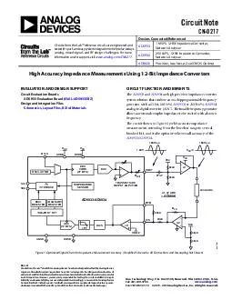
Circuit Note ��Rev. | Page of CIRCUIT DESCRIPTIONThe AD5933and AD5934have four programmable output voltageranges; each range has an output impedance associated with it. For example, the output impedance for a 1.98 V pp output voltageis typically 200 (see Table Table Output Series ResistanceOUTvs. Excitation Range for V= 3.3 V Supply Voltage RangeOutput ExcitationAmplitude(V pOutput ResistanceOUT Range 1 1.98 200 typ ical Range 20.97 2.4 k typical Range 30.3831.0 k typical Range 40.198 600 typical output impedance affectsthe impedancemeasurement accuracy, particularly in the low k range, and ustbe taken into account when calculating the gain factor. efer to the AD5933or AD5934data sheetfor more details on the gain factor calculation. A simplebuffer inthe signal chain preventthe output impedancefrom affectingthe unknown impedancemeasurementSelect alow output impedance amplifier with sufficient bandwidth to accommodate the AD5933AD5934excitationfrequency. An example of the low output impedance achievableis shownin Figure for the AD8605AD8606AD8608family of CMOS op amps.The output impedance for this amplifier for an Aof 1 is less than1 up to 100 kHz, which is the maximum operating range of theAD5933AD5934 FREQUENC (Hz) = 100 = 10 AV = 1 = 2.7V 09915-002OUTPUT IMPEDANCE (Ω) Figure . Output Impedance of AD8605AD8606AD8608 Matching the DC Bias of Transmit Stage to Receive StageThe four programmable output voltage ranges in the AD5933AD5934have four associated bias voltages (see Table ). For examplethe 1.98 V pp excitation voltage has a bias of 1.48 V. However, the currentvoltage (Ireceive stage of the AD5933AD5934set to a fixed bias of/2 as shown in Figure reforefor a 3.3 V supply, the transmit bias voltage is 1.48the receivebias voltage is 3.3 V/2 = 1.65 V. This potential differencepolarizesthe impedance under test and can cause inaccuracies in the impedance measurement.One solution is to add a simple highpass filter with a corner frequency in the low Hz range. Removing the dc bias from the transmit stage and rebiasing the ac signal to V/2 keeps the dc level constant throughout the signal chain. Table . Output Levels and Respective DC Bias for V= 3.3 VSupply VoltageRangeOutput ExcitationAmplitude(V pOutput DC Bias Level(V) 1 1.98 1.48 0.97 0.76 0.31 0.173 Selecting an Optimized IV Buffer for the Receive StageThe amplifier stage of the AD5933AD5934can also add minor inaccuracies to the signal chain. The IV conversion stage is sensitive to the amplifier's bias current, offset voltage, and commonmode rejection ratio (CMRR. By selecting the proper external discrete amplifier to perform the IV conversionthe user can choose an amplifier with lower bias current and offset voltage specifications along with excellent CMRR, makingthe IV conversion more accurate. The internal amplifier can then be configured as a simple inverting gain stage. Selection of the resistor still depends on the gain through the system as described in the AD5933AD5934data sheetOptimized Signal Chain for High Accuracy Impedance MeasurementsFigure shows a proposed configuration for measuring low impedance sensors. The ac signal is highpass filtered and rebiasedefore bufferingwith a very low output impedance amplifier. TheV conversion is completed externally before the signal returns to the AD5933AD5934receive stage. Key specifications that determine the required buffer are very low output impedance, the singlesupply capability, low bias current, low offset voltage, and excellent CMRR performance. Some suggested parts are the ADA4528AD8628AD8629, AD8605, and AD8606. Dependingon board layout, use a singlechannel or dualchannel amplifier. Useprecision 0.1% resistors for both the biasing resistors (50 k )and gain resistors (and R) to reduceinaccuracies. Circuit Note ��Rev. | Page of CIRCUIT EVALUATION AND TESTThe schematic in Figure was developed to improve impedance measurement accuracyand some example measurements were taken. The AD8606dualchannel amplifier bufferthe signalon the transmit pathand convertthe receive signal from current tooltage. For the three examples shown, the gain factor is calculatedfor each frequency increment to remove frequency dependent errors. A complete design package including schematicsbill of materials, layout, and Gerber files available for this solution at www.analog.com/CN0217DesignSupport. The software used is the same software that is available with evaluationboards and is accessible from the AD5933and AD5934product pages.Example 1: Low Impedance RangeTable . Low Impedance Range Setupfor V= 3.3 V Supply Voltage ParameterValue Voltage Peak - to - Peak (V p - p) 1.98 V (Range 1) Number of Settling Time Cycles MCLK16 MHz CAL20.1 20.0 Excitation Frequency Range 30 kHz to 30.2 kHz Unknown ImpedancesR1 = 10.3 , R2 = 30.0 C3 = 1 µF (Z= 5.3 at 30 kHz) The results of the low impedance measurements are shown in Figure Figure , and Figure Figure is for the 10.3 measurement and is shown on an expanded vertical scale. The accuracy achieved is very much dependent on howlarge theunknown impedance range is relative to the calibration resistor, CAL. Therefore, in this example, the unknown impedance of 10.3 measured 10.13, an approximate 2% error. Choosing an RCALcloser to the unknown impedance achieves a more accuratemeasurement; that is, the smaller the unknown impedance rangeis centered CALthe more accurate the measurement. Consequently, for large unknown impedance ranges, it is possibleto switch in various RCALresistors to break up the unknown impedance range using external switches. The Rerror of the switch is removed by calibration during the RCALgain factor calculation. Using a switch to select various Rvalues can optimize the dynamic range of the signal seen by the ADC.addition,note that toachieve a wider range of measurements mVp range was used. If the unknown Z is a small rangelarger output voltage range can be usedoptimizthe ADC dynamic range. 29.9530.0030.0530.1030.1530.2010.3Ω1µF30.25FREQUENCY (kHz)MAGNITUDE (Ω)09915-003 Figure . Measured Low Impedance Magnitude Results 29.9530.0030.0530.1030.1530.201µF30.25FREQUENCY (kHz)PHASE (Degrees)09915-004 10.3Ω, 30Ω Figure . Measued Low Impedance Phase Results 10.2210.2010.1810.1610.1410.1210.1010.0810.0610.0429.5030.0030.0530.1030.1530.2030.25FREQUENCY (kHz)MAGNITUDE (Ω)09915-005 Figure . Measured 10.3 Magnitude Results (Expanded Scale) Circuit Note ��Rev. | Page of Example 2: k Impedance RangeUsing an RCALof 99.85 k , a wide range of unknown impedanceswere measured according to the setup conditions listed inTable Figure to Figure document accuracy results. To improve the overall accuracy, select an RCALvalue closer to the unknown impedance. For example, in Figure an RCAL closer to the Zvalue of 217.5 k is required.If the unknown impedance range is large, use more than one RCALresistor. Table . k Impedance Range Setupfor V= 3.3 V Supply Voltage Parameter Value Voltage Peak - to - Peak (V p - p) 0.198 V (Range 4) Number of Settling Time Cycles MCLK16 MHz CAL99.85 k 100 k Excitation Frequency Range30 kHz to 50 kHz Unknown ImpedancesR0 = 99.85 kR1 = 29.88 k R2 = 14.95 k R3 = 8.21R4 = 217.25 k C5 = 150 pF= 26.5 kat 40kHz)C6 = 47pF (Z= 84.6 kat 40 kHz) FREQUENC (kHz)IMPEDANCE MAGNITUDE (kΩ)MEASUREDIDEA 09915-006 Figure Magnitude Result for = 47 pF, RCAL= 99.85 k –90.3–90.2–90.1–90.0–89.9–89.8–89.7–89.6–89.5–89.4–89.3FREQUENC (kHz)PHASE (Degrees) 09915-007 Figure Phase Resultor = 47 pF, RCAL= 99.85 k FREQUENC (kHz) IMPEDANCE MAGNITUDE (Ω) IDEA 09915-008 Figure = 8.21, R= 99.85 k FREQUENC (kHz)IMPEDANCE MAGNITUDE (kΩ)09915-009 213.5214.0214.521.50215.5216.0216.5217.0217.5218.0218.5 IDEA Figure = 217.5 k, RCAL= 99.85 k Circuit Note ��Rev. | Page of IMPEDANCE MAGNITUDE (kΩ)FREQUENC (kHz) 09915-010 Figure 10. Magnitude Results for Example 2: R1, R2, R3, C5, C6 Example 3: Parallel R||CMeasurementAn R||C type measurement was also made using the configurationsing an RCALof 1 k , an R of 10 k , and a C of 10 nF, measuracross a frequency range of 4 kHz to 100 kHz. The magnitude nd phase results videal are plotted in Figure and Figure Table R||CImpedance Range Setupfor V= 3.3 V Supply VoltageParameterValue Voltage Peak - to - Peak (V p - p) 0.383 V (Range 3) Number of Settling Time Cycles MCLK16 MHz CAL 1 k Excitation Fre quency Range 4 kHz to 100 kHz Unknown Impedance R||C R = 10 k , C = 10 n F IMPEDANCE MAGNITUDE (Ω)FREQUENC (kHz) IDEA MEASURED09915-0 Figure 11. Magnitude Results for = 10||10 nF, CAL FREQUENC (kHz) IDEA MEASUREDPHASE (Degrees) Figure 12. Phase Results for = 10||10 nF, CALetup and TestThevaluationboard software is he softwareused on the VALAD5933EBZefer to the technical note available on the CD provided with the evaluation board for details on the board setupNote that there are alterations to the schematic. Link nnectionson the VALAD5933EBZboard are listed in Table n addition,note that the location for Ris located at R3 on the evaluation boardand the location for ZUNKNOWNis C4.Table Link Connections for VALAD5933EBZLink NumberDefault Position LK1Open LK2Open LK3Insert LK4Open LK5Insert LK6 Complete setup and operation for the hardware and software for the evaluation board can be found in User Guide UGCOMMON VARIATIONSOther op ampcan be used in the circuit, such as the ADA4528AD8628AD8629AD8605, and AD8608Switching Options for System ApplicationsFor this particular circuit, the ZUNKNOWNand RCALwere interchangedanually. Howeverin production, use a low onresistance switchThe choice of the switch depends on how large the unknown impedance range is and how accurate the measurement result needs to be. The examples in his circuit noteuse just one calibration resistor, and so a low onresistance switchsuch as the ADG849can be used as shown in Figure . Multichannel switch solutionssuch as the quad ADG812can also be used. The errors caused by the switch resistance on the ZUNKNare removed during calibration, but by choosing a very low RON switch, the effects can be further minimized. Circuit Note ��Rev. | Page of UNKNOWNADG849 A1A2 09915–013 Figure 13Switching Between RCALand Unknown Z Using the ADG849Ultraow RSPDTSwitch (Simplified Schematic, All Connections and Decoupling Not Shown)LEARN MORE0217 Design Support Package: http://www.analog.com/CN0217DesignSupport085 Tutorial, "Fundamentals of Direct Digital Synthesis (DDS)," Analog Devices.Buchanan, David, "Choosing DACs for Direct Digital Synthesis," AN237 Application Note, Analog DevicesRiordan, Liam, "AD5933 Evaluation Board Example Measurement," AN1053 Application Note, Analog Devices.364 User Guide for AD5933 Evaluation BoardADIsimDDS Design and Evaluation ToolAD5933/AD5934 Demonstration and Design ToolData Sheets and Evaluation BoardsAD593Data SheetAD5933 Evaluation BoardAD5934 Data SheetAD5934 Evaluation BoardAD8606 Data SheetADG849 Data SheetADG812 Data SheetREVISION HISTORY3/13Rev. 0 to Rev. AUpdated Table Numbers; Renumbered SequentiallyChanges to Evaluation and Design Support SectionChanges to Setup and Test Section and Table 6Changes to Learn More Section/11Revision 0: Initial Version (Continued from first page) Circuits from the Lab circuits are intended only for use with Analo g Devices products and are the intellectual property of Analog Devices or its licensors. While you may use the Circuits from the Labcircuitsin the design of your product, no other license is granted by implication or otherwise under any patents or other intellectual property by application or use of the Circuits from the Labcircuits. Information furnished by Analog Devices is believed to be accurate and reliable. However, Circuits from the Labcircuitsare supplied "as is" and without warranties of any kind, express, implied, or statutory including, but not limited to, any implied warranty of merchantability, noninfringement or fitness for a particular purpose and no responsibility is assumed by Analog Devices for their use, nor for any infringements of patents or other rights of third parties that may result from their use. Analog Devices reserves the right to change any Circuits from the Lab circuits at any time without notice but is under no obligation to do so. 20112013Analog Devices, Inc. All rights reserved. Trademarks and registered trademarks are the property of their respective owners. CN099153/13(A) Circuit Note CN - 0217 Circuits from the Lab™ reference circuits are engineered andtested for quick and easy system integration to help solve today’s analog, mixedsignal, and RF design challenges. For more nformation and/or support, visitwww.analog.com/CN0217Devices Connected/Referenced AD59331 MSPS, Bit Impedance Converter, Network Analyzer AD5934250 kSPS, 12Bit Impedance Converter, Network Analyzer AD8606Precision, Low Noise, Dual CMOS Op Amp High Accuracy Impedance Measurements Using 12Bit Impedance Converters Rev. A Circuits from the Lab™ circuits from Analog Devices have been designed and built by Analog Devices engineers. Standard engineering practices have been employed in the design and construction of each circuit, and their function and performance have been tested and verified in a lab environment at room temperature. However, you are sol ely responsible for testing the circuit and determining its suitability and applicability for your use and application. Accordingly, in no event shall Analog Devices be liable for direct, indirect, special, incidental, consequential or punitive damages dueto any cause whatsoever connected to the use of any Circuits from the Lab circuits. (Continued on last page) One Technology Way, P.O. Box 9106, Norwood, MA 020629106, U.S.A.Tel: 781.329.4700www.analog.com Fax: 781.461.3113 © 2011 – 2013 Analog Devices, Inc. All rights reserved. EVALUATION AND DESIGN SUPPORT Circuit Evaluation BoardsAD5933Evaluation Board (EVALAD5933EBZ) Design and Integration Files Schematics, Layout Files, Bill of MaterialsRCUIT FUNCTION AND BENEFITSThe AD5933and AD5934are high precision impedance converter system solutions that combine an onchip programmable frequencygenerator with a bit, 1 MSPS (AD5933) or 250 kSPS (AD5934) analogtodigital converter (ADC). The tunable frequency generatorallows an external complex impedance to be excited with a knownfrequency. The circuit shown in Figure yields accurate impedance measurements extending from the low ohm range to several hundred k and it also optimizes the overall accuracy of the AD5933AD5934. 47nFUNKNOWN VDD ++ A1,A2AREAD8606 1.48V1.98V p-p 1.98V p-p VDD/2 DAC SCLSDA DVDD VDD MCLK AGND DGNDOUTVOUTAD5933/AD5934RFBVIN 1024-POINT DFT INTERIMAGINARYREGISTERREAREGISTEROSCILLATCORE(27 BITS) TEMPERATURESENSORTRANSMIT SIDEOUTPUTAMPLIFIER(12 BITS) LPFGAIN VDD VDD 09915-001I-V Figure . Optimized Signal Chain for Impedance Measurement Accuracy (Simplified Schematic, All Connections and Decoupling Not Shown)