
Change R18 value to 55kohm Add one 47uF bluk capacitor at output side in parallel with C10 to reduce the output ripple and improve load transient performance If the additional 47uF bulk capacitor is added at ID: 1030906
Download Presentation The PPT/PDF document "S chematic Add a 1uF/0402 ceramic capaci..." is the property of its rightful owner. Permission is granted to download and print the materials on this web site for personal, non-commercial use only, and to display it on your personal computer provided you do not modify the materials and that you retain all copyright notices contained in the materials. By downloading content from our website, you accept the terms of this agreement.


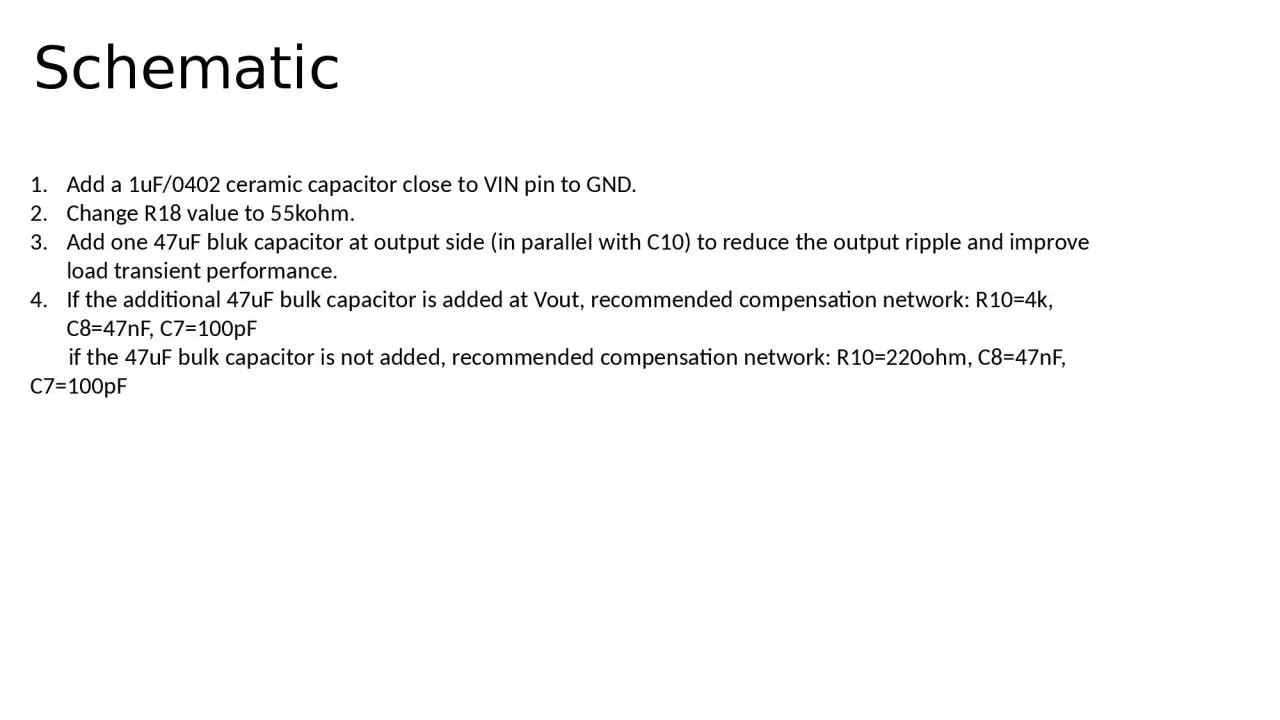
1. SchematicAdd a 1uF/0402 ceramic capacitor close to VIN pin to GND.Change R18 value to 55kohm.Add one 47uF bluk capacitor at output side (in parallel with C10) to reduce the output ripple and improve load transient performance.If the additional 47uF bulk capacitor is added at Vout, recommended compensation network: R10=4k, C8=47nF, C7=100pF if the 47uF bulk capacitor is not added, recommended compensation network: R10=220ohm, C8=47nF, C7=100pF
2. LayoutThe output capacitor should be put closer to IC Vout pin and PGND pin like C5 on EVM. The C5 GND terminal is connected to PGND pin directly on top layer.Add more VOUT vias on top of output capacitor C14
3. Connect the AGND plane to PGND plane at the GND terminal of VCC capacitor like EVM.
4. Fill this area with solid GND copper
5. Fill this area with solid Vout copper on top layer.