
6 432128121314151617182726 GNDV JT PACKAGEDW OR NT PACKAGETOP VIEWFK PACKAGETOP VIEW Q SDAS115C ID: 248895
Download Pdf The PPT/PDF document "QAQBQCQDQEQFQGQHCLKRCO" is the property of its rightful owner. Permission is granted to download and print the materials on this web site for personal, non-commercial use only, and to display it on your personal computer provided you do not modify the materials and that you retain all copyright notices contained in the materials. By downloading content from our website, you accept the terms of this agreement.

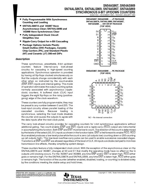
6 432128121314151617182726 GNDV QAQBQCQDQEQFQGQHCLKRCO ...JT PACKAGE...DW OR NT PACKAGE(TOP VIEW)...FK PACKAGE(TOP VIEW) Q SDAS115C ± DECEMBER 1982 ± REVISED JANUARY 1995 1995, Texas Instruments Incorporated POST OFFICE BOX 655303 DALLAS, TEXAS 75265Fully Programmable With Synchronous , ENT of operation eliminates the output counting spikesnormally associated with asynchronous (ripple-clock) counters. A buffered clock (CLK) inputThese counters are fully programmable; they maybe preset to any number between 0 and 255. Theload-input circuitry allows parallel loading of thecascaded counters. Because loading issynchronous, selecting the load mode disablesthe counter and causes the outputs to agree withThe carry look-ahead circuitry provides for cascading counters for n-bit synchronous applications withoutadditional gating. Two count-enable (ENP and ENT ) inputs and a ripple-carry (RCO in accomplishing this function. Both ENP and ENT must be low to count. The direction of the count is determined is fed forward to enable RCO . RCO thus enabled produces a low-level pulse while the count is zero (all outputs low) counting down or 255 countingup (all outputs high). This low-level overflow-carry pulse can be used to enable successive cascaded stages.Transitions at ENP and ENT are allowed regardless of the level of CLK. All inputs are diode clamped to minimizetransmission-line effects, thereby simplifying system design.These counters feature a fully independent clock circuit. With the exception of the asynchronous clear on theSN74ALS867A and AS867, changes at S0 and S1 that modify the operating mode have no effect on the Qoutputs until clocking occurs. For the and/or ENT is taken high, RCO eithergoes or remains high. For the SN74ALS867A and SN74ALS869, any time ENT is taken high, RCO either goesor remains high. The function of the counter (whether enabled, disabled, loading, or counting) is dictated solely PRODUCTION DATA information is current as of publication date.Products conform to specifications per the terms of Texas Instrumentsstandard warranty. Production processing does not necessarily includetesting of all parameters. SDAS115C ± DECEMBER 1982 ± REVISED JANUARY 1995 2 POST OFFICE BOX 655303 DALLAS, TEXAS 75265description (continued)The SN54AS867 and SN54AS869 are characterized for operation over the full military temperature range of±55FUNCTION TABLE S0 FUNCTION L L Clear L HCount down H LLoad H H Count up SN54AS867, SN54AS869 SN74ALS867A, SN74ALS869, SN74AS867, SN74AS869 SYNCHRONOUS 8-BIT UP/DOWN COUNTERS SDAS115C ± DECEMBER 1982 ± REVISED JANUARY 1995 3 POST OFFICE BOX 655303 DALLAS, TEXAS 75265logic symbols ENP CTRDIV 256 2,6D3A 4B 5C 6D 22 21 20 19 01S0 M 3 3,4CT=255 0R 7E 8F 9G 10H 18 17 16 15 12S1 G4 23 14CLK 131,4CT=0 RCO QAQBQCQDQEQFQGQHSN74ALS867AENT ENP CTRDIV 256 2,6D3A 4B 5C 6D 22 21 20 19 01S0 M 3 3,4CT=255 0,6R 7E 8F 9G 10H 18 17 16 15 12S1 G4 23 14CLK 131,4CT=0 RCO C6/1,4,5±/3,4,5+C6/1,4,5±/3,4,5+ These symbols are in accordance with ANSI/IEEE Std 91-1984 and IEC Publication 617-12.Pin numbers shown are for the DW, JT, and NT packages. SDAS115C ± DECEMBER 1982 ± REVISED JANUARY 1995 4 POST OFFICE BOX 655303 DALLAS, TEXAS 75265logic symbols (continued) ENP CTRDIV 256 2,6D3A 4B 5C 6D 22 21 20 19 01S0 M 3 3,4,5CT=255 0R 7E 8F 9G 10H 18 17 16 15 12S1 G4 23 14CLK 131,4,5CT=0 RCO QAQBQCQDQEQFQGQH4AS867ENT ENP CTRDIV 256 2,6D3A 4B 5C 6D 22 21 20 19 01S0 M 3 3,4,5CT=255 0,6R 7E 8F 9G 10H 18 17 16 15 12S1 G4 23 14CLK 131,4,5CT=0 RCO C6/1,4,5±/3,4,5+ C6/1,4,5±/3,4,5+ These symbols are in accordance with ANSI/IEEE Std 91-1984 and IEC Publication 617-12.Pin numbers shown are for the DW, JT, and NT packages. SN54AS867, SN54AS869 SN74ALS867A, SN74ALS869, SN74AS867, SN74AS869 SYNCHRONOUS 8-BIT UP/DOWN COUNTERS SDAS115C ± DECEMBER 1982 ± REVISED JANUARY 1995 5 POST OFFICE BOX 655303 DALLAS, TEXAS 75265logic diagram (positive logic) A 1DR C1 22 QA1412233B 1DR C1 21 QB4 C 1DR C1 20 QC5 D 1DR C1 19 QD6 E 1DR C1 18 QE7 ENP S1S0CLKF 1DR C1 17 QF8 G 1DR C1 16 QG9 H 1DR C1 15 QH10 13RCO ENT SN74ALS867A Only Pin numbers shown are for the DW, JT, and NT packages. SDAS115C ± DECEMBER 1982 ± REVISED JANUARY 1995 6 POST OFFICE BOX 655303 DALLAS, TEXAS 75265logic diagram (positive logic) 1DRC1 ENP S1S0CLKENT QARCO 121431322 1DRC1 QB421 1DRC1 QC520 1DRC1 QD619 1DRC1 QE718 AS867 Only 1DRC1 FQF817 1DRC1 QG916 1DRC1 QH1015 Pin numbers shown are for the DW, JT, and NT packages. SN54AS867, SN54AS869 SN74ALS867A, SN74ALS869, SN74AS867, SN74AS869 SYNCHRONOUS 8-BIT UP/DOWN COUNTERS SDAS115C ± DECEMBER 1982 ± REVISED JANUARY 1995 7 POST OFFICE BOX 655303 DALLAS, TEXAS 75265typical clear, preset, count, and inhibit sequences1.Clear outputs to zero (SN74ALS867A and 2.Preset to binary 2523.Count up to 253, 254, 255, 0, 1, and 24.Count down to 1, 0, 255, 254, 253, and 2525.Inhibit AsyncClearDEFCLKENP ENT QAQBQCQDRCO DataInputsOutputs QEQFQGQH Count Down GH B A S0 Preset SyncClear 25225325525425525425325201210 Count Up ²²ENT and ENP both must be low for counting to occur. SDAS115C ± DECEMBER 1982 ± REVISED JANUARY 1995 8 POST OFFICE BOX 655303 DALLAS, TEXAS 75265absolute maximum ratings over operating free-air temperature range (unless otherwise noted)Supply voltage, V . . . . . . . . . . . . . . . . . . . . : SN74ALS867A 0Storage temperature range ±65Stresses beyond those listed under ªabsolute maximum ratingsº may cause permanent damage to the device. These are stress ratings only, andfunctional operation of the device at these or any other conditions beyond those indicated under ªrecommended operating conditiimplied. Exposure to absolute-maximum-rated conditions for extended periods may affect device reliability.recommended operating conditions SN74ALS867A UNIT MIN NOM MAX UNIT V Supply voltage 4.5 5 5.5 V V High-level input voltage 2 V V Low-level input voltage 0.8 V I ±0.4 mA I Low-level output current 8 mA clock Clock frequency 0 35 MHz w(clock) Pulse duration, CLK high or low 14 ns w(clear) Pulse duration of clear pulse, S0 and S1 low 10 ns Data inputs A±H 10 ENP or ENT t Setup time before CLK=S0 low and S1 high (load) 12 ns S0 high and S1 low (count down) 12 S0 and S1 high (count up) 12 th HoldtimeafterCLK or S1 high after S0 3 ns t h H o ld t i me a f ter CLK= Data inputs A±H 0 ns TA Operating free-air temperature 0 70 5C electrical characteristics over recommended operating free-air temperature range (unlessotherwise noted) PARAMETER TESTCONDITIONS SN74ALS867A UNIT PARAMETER TEST CONDITIONS MIN TYP³ MAX UNIT V = 4.5 V, = ±18 mA ±1.2 V V = 4.5 V to 5.5 V, = ±0.4 mA ±2 V V =45V I = 4 mA 0.4 V V V = 4 . 5 V I = 8 mA 0.5 V II = 5.5 V, VI = 7 V mA I = 5.5 V, = 2.7 V 20 mA I = 5.5 V, = 0.4 V ±0.2 mA IO§ = 5.5 V, = 2.25 V ±30 ±112 mA I = 5.5 V 28 45 mA = 5 V, T = 25 current, I SN54AS867, SN54AS869 SN74ALS867A, SN74ALS869, SN74AS867, SN74AS869 SYNCHRONOUS 8-BIT UP/DOWN COUNTERS SDAS115C ± DECEMBER 1982 ± REVISED JANUARY 1995 9 POST OFFICE BOX 655303 DALLAS, TEXAS 75265switching characteristics (see Figure 1)PARAMETER FROM ( INPUT ) ( ) = 4.5 V to 5.5 V, = 50 pF, = 500 UNIT (INPUT) (OUTPUT) SN74ALS867A MIN MAX f MHz t 4 ns tPHL CLK RCO 4 14 ns t AnyQ 3 ns tPHL CLK An y Q 3 16 ns t 3 ns tPHL ENT RCO 2 9 ns tPHL S0 or S1 (clear mode) Any Q 8 26 ns t S0 or S1 RCO 4 16 ns tPHL (count up/down) RCO 4 16 ns t S0 or S1 (clear mode) RCO 4 16 ns ²For conditions shown as MIN or MAX, use the appropriate value specified under recommended operating conditions. SDAS115C ± DECEMBER 1982 ± REVISED JANUARY 1995 10 POST OFFICE BOX 655303 DALLAS, TEXAS 75265absolute maximum ratings over operating free-air temperature range (unless otherwise noted)Supply voltage, V . . . . . . . . . . . . . . . . . . . . : SN74ALS869 0Storage temperature range ±65Stresses beyond those listed under ªabsolute maximum ratingsº may cause permanent damage to the device. These are stress ratings only, andfunctional operation of the device at these or any other conditions beyond those indicated under ªrecommended operating conditiimplied. Exposure to absolute-maximum-rated conditions for extended periods may affect device reliability.recommended operating conditions SN74ALS869 UNIT MIN NOM MAX UNIT V Supply voltage 4.5 5 5.5 V V High-level input voltage 2 V V Low-level input voltage 0.8 V I ±0.4 mA I Low-level output current 8 mA clock Clock frequency 0 35 MHz w(clock) Pulse duration, CLK high or low 14 ns Data inputs A±H 10 ENP or ENT t SetptimebeforeCLK S0 and S1 low (clear) 13 ns t S etup t i me b e f ore CLK= S0 low and S1 high (load) 13 ns S0 high and S1 low (count down) 13 S0 and S1 high (count up) 13 th HoldtimeafterCLK or S1 high after S0 3 ns t h H o ld t i me a f ter CLK= Data inputs A±H 0 ns TA Operating free-air temperature 0 70 5C electrical characteristics over recommended operating free-air temperature range (unlessotherwise noted) PARAMETER TESTCONDITIONS SN74ALS869 UNIT PARAMETER TEST CONDITIONS MIN TYP³ MAX UNIT V = 4.5 V, = ±18 mA ±1.2 V V = 4.5 V to 5.5 V, = ±0.4 mA ±2 V V =45V I = 4 mA 0.4 V V V = 4 . 5 V I = 8 mA 0.5 V II = 5.5 V, VI = 7 V mA I = 5.5 V, = 2.7 V 20 mA I = 5.5 V, = 0.4 V ±0.2 mA IO§ = 5.5 V, = 2.25 V ±30 ±112 mA I = 5.5 V 28 45 mA = 5 V, T = 25 current, I SN54AS867, SN54AS869 SN74ALS867A, SN74ALS869, SN74AS867, SN74AS869 SYNCHRONOUS 8-BIT UP/DOWN COUNTERS SDAS115C ± DECEMBER 1982 ± REVISED JANUARY 1995 POST OFFICE BOX 655303 DALLAS, TEXAS 75265switching characteristics (see Figure 1)PARAMETER FROM ( INPUT ) ( ) = 4.5 V to 5.5 V, = 50 pF, = 500 UNIT (INPUT) (OUTPUT) SN74ALS869 MIN MAX f MHz t 4 ns tPHL CLK RCO 4 14 ns t AnyQ 3 ns tPHL CLK An y Q 3 16 ns t 3 ns tPHL ENT RCO 2 9 ns t RCO 4 15 ns tPHL (count up/down) RCO 4 15 ns t RCO 4 16 ns tPHL (clear/load) RCO 4 12 ns ²For conditions shown as MIN or MAX, use the appropriate value specified under recommended operating conditions. SDAS115C ± DECEMBER 1982 ± REVISED JANUARY 1995 12 POST OFFICE BOX 655303 DALLAS, TEXAS 75265absolute maximum ratings over operating free-air temperature range (unless otherwise noted)Supply voltage, V . . . . . . . . . . . . . . . . . . . . :SN54AS867 ±55SN74AS867 0Storage temperature range ±65Stresses beyond those listed under ªabsolute maximum ratingsº may cause permanent damage to the device. These are stress ratings only, andfunctional operation of the device at these or any other conditions beyond those indicated under ªrecommended operating conditiimplied. Exposure to absolute-maximum-rated conditions for extended periods may affect device reliability.recommended operating conditions SN54AS867 SN74AS867 UNIT MIN NOM MAX MIN NOM MAX UNIT V Supply voltage 4.5 5 5.5 4.5 5 5.5 V V High-level input voltage 2 2 V V Low-level input voltage 0.8 0.8 V I ±2 I Low-level output current 20 20 mA clock Clock frequency 0 40 0 50 MHz w(clock) Pulse duration, CLK high or low 12.5 10 ns w(clear) Pulse duration of clear pulse, S0 and S1 low 12.5 10 ns Data inputs A±H 5 4 ENP or ENT 9 8 t * SetptimebeforeCLK S0 low and S1 high (load) ns t * S etup t i me b e f ore CLK= S0 and S1 low (clear) ns S0 high and S1 low (count down) 42 40 S0 and S1 high (count up) 42 40 th* Hold time after CLK= Data inputs A±H 0 0 ns skew (maximum to avoid inadvertent clear) 8 7 ns TA Operating free-air temperature ±55 0 70 5C * On products compliant to MIL-STD-883, Class B, this parameter is based on characterization data but is not production tested. SN54AS867, SN54AS869 SN74ALS867A, SN74ALS869, SN74AS867, SN74AS869 SYNCHRONOUS 8-BIT UP/DOWN COUNTERS SDAS115C ± DECEMBER 1982 ± REVISED JANUARY 1995 13 POST OFFICE BOX 655303 DALLAS, TEXAS 75265electrical characteristics over recommended operating free-air temperature range (unlessotherwise noted) PARAMETER TESTCONDITIONS SN54AS867 SN74AS867 UNIT PARAMETER TEST CONDITIONS MIN TYP² MAX MIN TYP² MAX UNIT V = 4.5 V, = ±18 mA ±1.2 ±1.2 V V = 4.5 V to 5.5 V, = ±2 mA ±2 ±2 V V V = 4.5 V = 20 mA, on ENT = 0.7 V 0.34 0.5 V Other outputs = 20 mA 0.34 0.5 II = 5.5 V, VI = 7 V 0.1 mA I ENT =55V =27V 40 40 mA I Other inputs V = 5 . 5 V , V = 2 . 7 V 20 20 m A I ENT =55V =04V ±4 I Other inputs V = 5 . 5 V , V = 0 . 4 V ±2 IO³ = 5.5 V, = 2.25 V ±30 ±112 ±30 ±112 I = 5.5 V 134 195 134 195 mA = 5 V, T = 25 current, Iswitching characteristics (see Figure 1)PARAMETER FROM ( INPUT ) ( ) = 4.5 V to 5.5 V, = 50 pF, = 500 UNIT (INPUT) (OUTPUT) SN54AS867 SN74AS867 MIN MAX MIN MAX f* 50 MHz t 5 5 22 ns tPHL CLK RCO 6 19 6 16 ns t AnyQ 3 3 t CLK An y Q 4 16 4 15 ns t 3 3 10 ns tPHL ENT RCO 5 21 5 17 ns t 5 5 14 ns tPHL ENP RCO 5 21 5 17 ns tPHL Clear (S0 or S1 low) Any Q 7 23 7 21 ns * On products compliant to MIL-STD-883, Class B, this parameter is based on characterization data but is not production tested.§For conditions shown as MIN or MAX, use the appropriate value specified under recommended operating conditions. SDAS115C ± DECEMBER 1982 ± REVISED JANUARY 1995 14 POST OFFICE BOX 655303 DALLAS, TEXAS 75265absolute maximum ratings over operating free-air temperature range (unless otherwise noted)Supply voltage, V . . . . . . . . . . . . . . . . . . . . :SN54AS869 ±55SN74AS869 0Storage temperature range ±65Stresses beyond those listed under ªabsolute maximum ratingsº may cause permanent damage to the device. These are stress ratings only, andfunctional operation of the device at these or any other conditions beyond those indicated under ªrecommended operating conditiimplied. Exposure to absolute-maximum-rated conditions for extended periods may affect device reliability.recommended operating conditions SN54AS869 SN74AS869 UNIT MIN NOM MAX MIN NOM MAX UNIT V Supply voltage 4.5 5 5.5 4.5 5 5.5 V V High-level input voltage 2 2 V V Low-level input voltage 0.7 0.8 V I ±2 I Low-level output current 20 20 mA clock Clock frequency 40 45 MHz w(clock) Pulse duration, CLK high or low 12.5 Data inputs A±H 6 5 ENP or ENT 9 t * SetptimebeforeCLK S0 low and S1 high (load) 13 t * S etup t i me b e f ore CLK= S0 and S1 low (clear) 13 S0 high and S1 low (count down) 52 50 S0 and S1 high (count up) 52 50 th* Hold time after CLK= Data inputs A±H 0 0 ns TA Operating free-air temperature ±55 0 70 5C * On products compliant to MIL-STD-883, Class B, this parameter is based on characterization data but is not production tested. SN54AS867, SN54AS869 SN74ALS867A, SN74ALS869, SN74AS867, SN74AS869 SYNCHRONOUS 8-BIT UP/DOWN COUNTERS SDAS115C ± DECEMBER 1982 ± REVISED JANUARY 1995 15 POST OFFICE BOX 655303 DALLAS, TEXAS 75265electrical characteristics over recommended operating free-air temperature range (unlessotherwise noted) PARAMETER TESTCONDITIONS SN54AS869 SN74AS869 UNIT PARAMETER TEST CONDITIONS MIN TYP² MAX MIN TYP² MAX UNIT V = 4.5 V, = ±18 mA ±1.2 ±1.2 V V = 4.5 V to 5.5 V, = ±2 mA ±2 V V = 4.5 V, = ±2 mA ±2* V V V = 4.5 V = 20 mA, on ENT = 0.7 V 0.34 0.5 V Other outputs = 20 mA 0.34 0.5 II = 5.5 V, VI = 7 V 0.1 mA I ENT =55V =27V 40 40 mA I Other inputs V = 5 . 5 V , V = 2 . 7 V 20 20 m A I ENT =55V =04V ±4 I Other inputs V = 5 . 5 V , V = 0 . 4 V ±2 IO³ = 5.5 V, = 2.25 V ±30 ±112 ±30 ±112 I = 5.5 V 134 195 134 195 mA = 5 V, T = 25 current, Iswitching characteristics (see Figure 1)PARAMETER FROM ( INPUT ) ( ) = 4.5 V to 5.5 V, = 50 pF, = 500 UNIT (INPUT) (OUTPUT) SN54AS869 SN74AS869 MIN MAX MIN MAX f* 45 MHz t 6 6 35 ns tPHL CLK RCO 6 20 6 18 ns t AnyQ 3 3 t CLK An y Q 4 16 4 15 ns t 3 3 15 ns tPHL ENT RCO 6 21 6 17 ns t 5 5 19 ns tPHL ENP RCO 6 21 6 18 ns * On products compliant to MIL-STD-883, Class B, this parameter is based on characterization data but is not production tested.§For conditions shown as MIN or MAX, use the appropriate value specified under recommended operating conditions. SDAS115C ± DECEMBER 1982 ± REVISED JANUARY 1995 16 POST OFFICE BOX 655303 DALLAS, TEXAS 75265PARAMETER MEASUREMENT INFORMATIONSERIES 54ALS/74ALS AND 54AS/74AS DEVICES 0.3 VFOR 3-STATE OUTPUTSUnder Test Test VOLTAGE WAVEFORMSTiming 1.3 V1.3 V VOLTAGE WAVEFORMSPULSE DURATIONS 1.3 V1.3 V1.3 V1.3 VWaveform 1Waveform 21.3 V1.3 V VOLTAGE WAVEFORMSPROPAGATION DELAY TIMESVOLTAGE WAVEFORMSENABLE AND DISABLE TIMES, 3-STATE OUTPUTS Test Under TestFOR OPEN-COLLECTOR OUTPUTS BI-STATETOTEM-POLE OUTPUTSUnder Test Test RL RL = R1 = R2 NOTES:A.C includes probe and jig capacitance.B.Waveform 1 is for an output with internal conditions such that the output is low except when disabled by the output control.Waveform 2 is for an output with internal conditions such that the output is high except when disabled by the output control.C.When measuring propagation delay items of 3-state outputs, switch S1 is open.D.All input pulses have the following characteristics: PRR E.The outputs are measured one at a time with one transition per measurement.Figure 1. Load Circuits and Voltage Waveforms PACKAGE OPTION ADDENDUM www.ti.com 28-Jul-2020 Addendum-Page 1 PACKAGING INFORMATION Orderable Device Status(1) Package Type PackageDrawing Pins PackageQty Eco Plan(2) Lead finish/Ball material(6) MSL Peak Temp(3) Op Temp (°C) Device Marking(4/5) Samples 5962-8952601LA ACTIVE CDIP JT 24 1 TBD SNPB N / A for Pkg Type -55 to 125 5962-8952601LASNJ54AS869JT 5962-8966801LA ACTIVE CDIP JT 24 1 TBD SNPB N / A for Pkg Type -55 to 125 5962-8966801LASNJ54AS867JT SN54AS867JT ACTIVE CDIP JT 24 1 TBD SNPB N / A for Pkg Type -55 to 125 SN54AS867JT SN54AS869JT ACTIVE CDIP JT 24 1 TBD SNPB N / A for Pkg Type -55 to 125 SN54AS869JT SN74ALS867ADW ACTIVE SOIC DW 24 25 Green (RoHS& no Sb/Br) NIPDAU Level-1-260C-UNLIM 0 to 70 ALS867A SN74ALS869DW ACTIVE SOIC DW 24 25 Green (RoHS& no Sb/Br) NIPDAU Level-1-260C-UNLIM 0 to 70 ALS869 SN74ALS869DWE4 ACTIVE SOIC DW 24 25 Green (RoHS& no Sb/Br) NIPDAU Level-1-260C-UNLIM 0 to 70 ALS869 SN74AS867DW ACTIVE SOIC DW 24 25 Green (RoHS& no Sb/Br) NIPDAU Level-1-260C-UNLIM 0 to 70 AS867 SN74AS869DW ACTIVE SOIC DW 24 25 Green (RoHS& no Sb/Br) NIPDAU Level-1-260C-UNLIM 0 to 70 AS869 SNJ54AS867JT ACTIVE CDIP JT 24 1 TBD SNPB N / A for Pkg Type -55 to 125 5962-8966801LASNJ54AS867JT SNJ54AS869JT ACTIVE CDIP JT 24 1 TBD SNPB N / A for Pkg Type -55 to 125 5962-8952601LASNJ54AS869JT (1) The marketing status values are defined as follows: ACTIVE: Product device recommended for new designs. LIFEBUY: TI has announced that the device will be discontinued, and a lifetime-buy period is in effect. NRND: Not recommended for new designs. Device is in production to support existing customers, but TI does not recommend using this part in a new design. PREVIEW: Device has been announced but is not in production. Samples may or may not be available. OBSOLETE: TI has discontinued the production of the device. (2) RoHS: TI defines "RoHS" to mean semiconductor products that are compliant with the current EU RoHS requirements for all 10 RoHS substances, including the requirement that RoHS substancedo not exceed 0.1% by weight in homogeneous materials. Where designed to be soldered at high temperatures, "RoHS" products are suitable for use in specified lead-free processes. TI mayreference these types of products as "Pb-Free". RoHS Exempt: TI defines "RoHS Exempt" to mean products that contain lead but are compliant with EU RoHS pursuant to a specific EU RoHS exemption. Green: TI defines "Green" to mean the content of Chlorine (Cl) and Bromine (Br) based flame retardants meet JS709B low halogen requirements of threshold. Antimony trioxide basedflame retardants must also meet the threshold requirement. PACKAGE OPTION ADDENDUM www.ti.com 28-Jul-2020 Addendum-Page 2 (3) MSL, Peak Temp. - The Moisture Sensitivity Level rating according to the JEDEC industry standard classifications, and peak solder temperature. (4) There may be additional marking, which relates to the logo, the lot trace code information, or the environmental category on the device. (5) Multiple Device Markings will be inside parentheses. Only one Device Marking contained in parentheses and separated by a "~" will appear on a device. If a line is indented then it is a continuationof the previous line and the two combined represent the entire Device Marking for that device. (6) Lead finish/Ball material - Orderable Devices may have multiple material finish options. Finish options are separated by a vertical ruled line. Lead finish/Ball material values may wrap to twolines if the finish value exceeds the maximum column width. Important Information and Disclaimer:The information provided on this page represents TI's knowledge and belief as of the date that it is provided. TI bases its knowledge and belief on informationprovided by third parties, and makes no representation or warranty as to the accuracy of such information. Efforts are underway to better integrate information from third parties. TI has taken andcontinues to take reasonable steps to provide representative and accurate information but may not have conducted destructive testing or chemical analysis on incoming materials and chemicals.TI and TI suppliers consider certain information to be proprietary, and thus CAS numbers and other limited information may not be available for release. In no event shall TI's liability arising out of such information exceed the total purchase price of the TI part(s) at issue in this document sold by TI to Customer on an annual basis. OTHER QUALIFIED VERSIONS OF SN54AS867, SN54AS869, SN74AS867, SN74AS869 :•Catalog: SN74AS867, SN74AS869•Military: SN54AS867, SN54AS869 NOTE: Qualified Version Definitions:•Catalog - TI's standard catalog product•Military - QML certified for Military and Defense Applications MECHANICAL DATA MCER004A ± JANUARY 1995 ± REVISED JANUARY 1997 POST OFFICE BOX 655303 JT (R-GDIP-T**)CERAMIC DUAL-IN-LINE 24 LEADS SHOWN4040110/C 08/96 B 0.200 (5,08) MAX 0.320 (8,13)0.290 (7,37) 0.130 (3,30) MIN 0.008 (0,20)0.014 (0,36)Seating Plane 13 12 0.030 (0,76)0.070 (1,78) 0.015 (0,38) MIN A 24 1 0.100 (2,54) MAX 0.023 (0,58)0.015 (0,38) 0.100 (2,54) 05±155 1.440(37,08) 1.460 0.285(7,39) 0.291(36,58)(7,24) 28PINS ** 1.280 1.240 0.300(7,62)DIMB MAXA MAXA MINB MIN(6,22) 24 (32,51) NOTES:A.All linear dimensions are in inches (millimeters).B.This drawing is subject to change without notice.C.This package can be hermetically sealed with a ceramic lid using glass frit.D.Index point is provided on cap for terminal identification.E.Falls within MIL STD 1835 GDIP3-T24, GDIP4-T28, and JEDEC MO-058 AA, MO-058 AB IMPORTANTNOTICEANDDISCLAIMER “ASIS”