
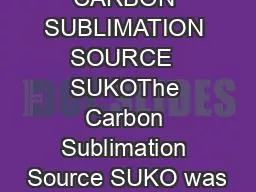
Ptype doping concentration for bulk and delta doping in GaAs as a function of the electrical current of a SUKO 40 4Front view of hot carbon x00660069 lament operation after removal Excellent ID: 819242
Download Pdf The PPT/PDF document "CARBON SUBLIMATION SOURCE SUKOThe Carbo..." is the property of its rightful owner. Permission is granted to download and print the materials on this web site for personal, non-commercial use only, and to display it on your personal computer provided you do not modify the materials and that you retain all copyright notices contained in the materials. By downloading content from our website, you accept the terms of this agreement.


CARBON SUBLIMATION SOURCE SUKOThe Carbo
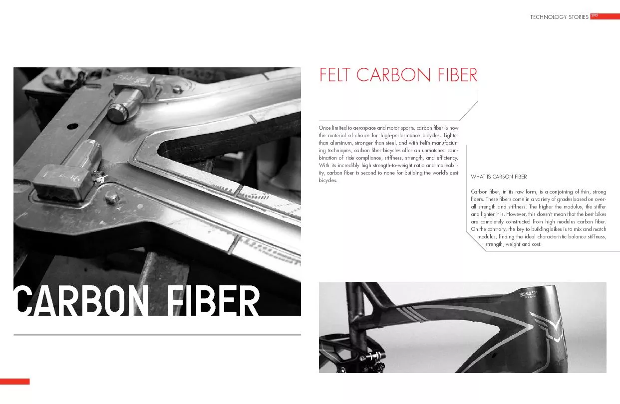
CARBON SUBLIMATION SOURCE SUKOThe Carbon Sublimation Source SUKO was developed for growth of Si-C and Si-Ge-C alloys in Si MBE. Providing a very clean and constant � ux at a low deposition rate up to 2 Å/min a maximum total layer thickness of 5 µm of C with one � lament is achieved. A more recent application of the SUKO is the preparation of high purity graphene O is the preparation of high purity graphene The new SUKO-D version is an optimized doping source for carbon p-type doping in III-V MBE. It has been carefully redesigned for low power consumption in collaboration with Prof. W. Wegscheider, formerly P-type doping concentration for bulk and delta doping in GaAs as a function of the electrical current of a SUKO 40 [4].Front view of hot carbon � lament (operation after removal Excellent growth of thin carbon � lms in III-V MBE� lamentLow power consumptionNo ceramic parts or metal parts sublimating � lamentDr. Eberl MBE-Komponenten GmbH Josef-Beyerle-Str. 18/171263 Weil der Stadt, GermanyFon Webwww.mbe-components.com bulk p-type doping applications the hole mobility turns out to be comparable to mobilities achieved by Be doping. The advantage of C-doping is the lower diffusion of C-atoms compared to Be-atoms. Optical, REM and xstudies have all con�rmed the excellent morphology of the layers. In contrast to carbon gas source
s no interaction with MBE equipment or m
s no interaction with MBE equipment or memory effect is observed while operating the SUKO-D. Record hole mobilities in high mobility MBE systems of 1.2x10/Vs in GaAs/AlGaAs hetero structures at a carrier density of 2.3x10Technical DataMounting �ange DN40CF (O.D. 2.75“) for SUKO 40 / SUKO-D 40 DN63CF (O.D. 4.5“) for SUKO 63 length: 216 - 400 mm; ØD: 36 mm for SUKO 40 / SUKO-D 40length: 216 - 400 mm; ØD: 55 mm for SUKO 63 max. current 65 A for C-doping with SUKO-D 40 max. current 75 A; max �ux 0.5 Å/min for SUKO 40 max. current 100 A; max �ux 2 Å/min; for SUKO 63 Bakeout temperature integrated rotary shutter (S) (for SUKO 63 only; ØD: 62 mm)[1] Carbon doped symmetric GaAs/AlGaAs quantum wells with hole mobilities beyond 10/Vs; C. Gerl, S. Schmult, H.-P. Tranitz, C.Mitzkus, W. Wegscheider; Appl. Phys. Lett. 86 25,2105; 86 20,2105 (2005) [2] Heavy carbon doping of GaAs grown by solid source molecular-beam epitaxy; C. Cianni, A. Fischer, C. Lange, K. Ploog and L. Tapfer, Appl. Phys. Lett. (1992)Achievable doping levels with a SUKO source [2] are: P-doping GaAs 6.5x10, with a mobility of 29 cm²/Vs (measured at 300 K). The maximum bulk doping level of GaAlAs (35% Al, thickness 1500 Å) is 7.5x10 The maximum delta doping level in GaAs is 2x10 Minority carrier lifetime in p-doped GaAs (1.7x10Carbon Sublimation Source SUKOSUKO 63-S with shutte