
Prototype Showcase What is a metamaterial How our 2D sample was created How our phase mask was created SEM images of 2D sample and phase mask Metamaterials A periodic material that has photonic or phononic properties ID: 414527
Download Presentation The PPT/PDF document "Metamaterials" is the property of its rightful owner. Permission is granted to download and print the materials on this web site for personal, non-commercial use only, and to display it on your personal computer provided you do not modify the materials and that you retain all copyright notices contained in the materials. By downloading content from our website, you accept the terms of this agreement.


Slide1
MetamaterialsSlide2
Prototype Showcase
What is a metamaterial?
How our 2-D sample was created
How our phase mask was created
SEM images of 2-D sample and phase maskSlide3
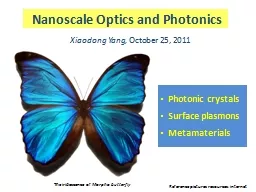
Metamaterials
A periodic material that has photonic or phononic properties.
*Taken From 3.042 handout & Physics Worlds 2005 “Sound Ideas”Slide4
Deliverables
3-D periodic structure with micro-scale periodicity
Macro-scale representations of the structuresSlide5
Prototype Design
2-D structure
phase mask
3-D structure
2-D structure:
2 microns thick,5 microns thick,
15 microns thick
Variable spacing
3-D structure:
Very thick (~50 microns)
Variable spacingSlide6
Contact Lithography
Coat
Exposure
Develop
plain Si wafer
coat with HMDS to make Si wafer hydrophobic
coat with SU-8 2015 photoresist using spin coater
soft bake @95° to evaporate solvent and cut into pieces
UV exposure for either 15, 20, 25, or 30 seconds
flip 90° and expose again
post bake at first 65° then 95° to promote crosslink formation
submerge in PM acetate to dissolve unexposed photoresist (20 min
)
submerge in isopropanol to wash away all remnants—final structureSlide7
Phase mask
Step 1
Step 2
Step 3
Vacuum sample with open bottle of fluorosilane so that it evaporates onto sample.
Layer with PDMS and heat at 65°to 75°for at least three hours.
Gently peel off PDMS
layer as phase mask.Slide8
Fabrication and Processing
SU-8 2002:
15 seconds,
20 seconds,
25 seconds
SU-8 2005:
25 seconds,
30 seconds,
35 seconds,
40 seconds
SU-8 2015:
15 seconds,
20 seconds,
25 seconds,
30 seconds,
35 seconds,
40 seconds,
45 seconds
Type of PhotoresistSlide9
Prototype Functionality
Thick Film Photoresist
Sin (70) = 58 / t
Calculation:
Thickness (t) ~ 61 microns
Success!Slide10
Prototype Functionality
2-D Patterns
Top-down view:
Hole Spacing ~
3.38 um
Hole Length ~
1.56 um
Hole Height ~
1.54 um
Cross-section view:
Width of top ~
1.81 um
Width of bottom ~
1.00 um
Height ~
10.00 umSlide11
Prototype Functionality
Problems in 2-D patterns
Over exposure
Un-washed monomer
Non-uniform columns
Width of top ~
1.81 um
Width of bottom ~
1.00 umSlide12
Prototype Functionality
Phase maskSlide13
?
2-D Pattern
Phase Mask
3-D Pattern
CAD Model
3-D Printing Model
Actual SampleSlide14Slide15
Questions?