
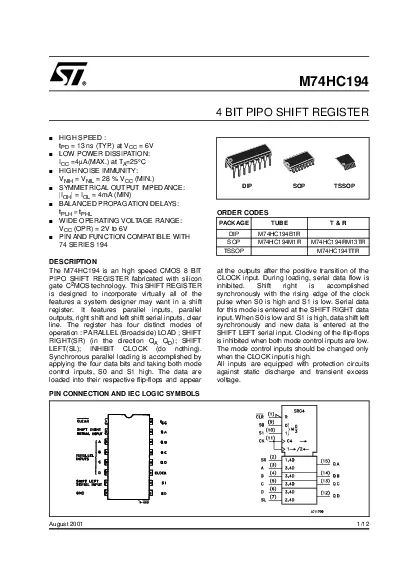
112PIN CONNECTION AND IEC LOGIC SYMBOLSORDER CODES PACKAGETUBET RDIPM74HC194B1RSOPM74HC194M1RM74HC194RM13TRTSSOPM74HC194TTRTSSOPDIPSOPM74HC194212INPUT AND OUTPUT EQUIVALENT CIRCUIT PIN DESCRIPT ID: 862128
Download Pdf The PPT/PDF document "August 2001HIGH SPEED 13 ns TYP at VL..." is the property of its rightful owner. Permission is granted to download and print the materials on this web site for personal, non-commercial use only, and to display it on your personal computer provided you do not modify the materials and that you retain all copyright notices contained in the materials. By downloading content from our website, you accept the terms of this agreement.


1 1/12 August 2001HIGH SPEED : = 13 ns (T
1/12 August 2001HIGH SPEED : = 13 ns (TYP.) at VLOW POWER DISSIPATION:A(MAX.) at T=25°CHIGH NOISE IMMUNITY:NIH = VNIL = 28 % V (MIN.)SYMMETRICAL OUTPUT IMPEDANCE:| = I = 4mA (MIN)BALANCED PROPAGATION DELAYS:PLHWIDE OPERATING VOLTAGE RANGE: (OPR) = 2V to 6VPIN AND FUNCTION COMPATIBLE WITH 74 SERIES 194DESCRIPTIONThe M74HC194 is an high speed CMOS 8 BITPIPO SHIFT REGISTER fabricated with silicongate CMOS technology. This SHIFT REGISTERis designed to incorporate virtually all of thefeatures a system designer may want in a shiftregister. It features parallel inputs, paralleloutputs, right shift and left shift serial inputs
2 , clearline. The register has four disti
, clearline. The register has four distinct modes ofoperation : PARALLEL (Broadside) LOAD ; SHIFTRIGHT(SR) (in the direction Q); SHIFTLEFT(SL); INHIBIT CLOCK (do nothing).Synchronous parallel loading is accomplished byapplying the four data bits and taking both modecontrol inputs, S0 and S1 high. The data areloaded into their respective flip-flops and appearat the outputs after the positive transition of theCLOCK input. During loading, serial data flow isinhibited. Shift right is accomplishedsynchronously with the rising edge of the clockpulse when S0 is high and S1 is low. Serial datafor this mode is entered at the SHIFT
3 RIGHT datainput. When S0 is low and S1
RIGHT datainput. When S0 is low and S1 is high, data shift leftsynchronously and new data is entered at theSHIFT LEFT serial input. Clocking of the flip-flopsis inhibited when both mode control inputs are low.The mode control inputs should be changed onlywhen the CLOCK input is high.All inputs are equipped with protection circuitsagainst static discharge and transient excessvoltage.M74HC1944 BIT PIPO SHIFT REGISTER PIN CONNECTION AND IEC LOGIC SYMBOLSORDER CODES PACKAGETUBET & RDIPM74HC194B1RSOPM74HC194M1RM74HC194RM13TRTSSOPM74HC194TTR TSSOP DIPSOP M74HC194 2/12 INPUT AND OUTPUT EQUIVALENT CIRCUIT PIN DESCRIPTION
4 TRUTH TABLE X : Dont Carea ~ d
TRUTH TABLE X : Dont Carea ~ d : The level of steady state input voltage at input A ~ DQA0 ~ QD0 : No ChangeQAn ~ QDn : The level of QA, QB, QC, respectively, before the most recent positive transition of the clock. PIN NoSYMBOLNAME AND FUNCTION1CLEAR Asynchronous Reset Input (Active LOW)Serial Data Input (Shift Right)3, 4, 5, 6A to DParallel Data InputsSerial Data Input (Shift Left)9, 10S0, S1Mode Control Inputs11CLOCKClock Input (LOW to HIGH Edge-triggered)15, 14, 13, QA to QD Parallel Outputs8GNDGround (0V)16VccPositive Supply Voltage INPUTSOUTPUTSCLEAR MODECLOCKSERIALPARALLELQAQBQCQDS1S
5 0LEFTRIGHTABCDLXXXXXXXXXLLLLHXXXXXXXXQA0
0LEFTRIGHTABCDLXXXXXXXXXLLLLHXXXXXXXXQA0QB0QC0QD0HHHXXabcdabcdHLHXHXXXXHQAnQBnQCnHLHXLXXXXLQAnQBnQCnHHLHXXXXXQBnQCnQDnHHHLLXXXXXQBnQCnQDnLHLLXXXXXXXQA0QB0QC0QD0 M74HC194 3/12 LOGIC DIAGRAM This logic diagram has not be used to estimate propagation delaysTIMING CHART M74HC194 4/12 ABSOLUTE MAXIMUM RATINGS Absolute Maximum Ratings are those values beyond which damage to the device may occur. Functional operation under these conditions is not implied(*) 500mW at 65 C; derate to 300mW by 10mW/C from 65C to 85RECOMMENDED OPERATING CONDITIONS SymbolParameterValueUnitSupply Voltage-0.5 to +7VDC Input Voltage-0.5 to V
6 + 0.5DC Output Voltage-0.5 to V + 0.5DC
+ 0.5DC Output Voltage-0.5 to V + 0.5DC Input Diode Current 20mADC Output Diode Current 20mADC Output Current 25mA or IGND or Ground Current 50mAPower Dissipation500(*)mWstgStorage Temperature-65 to +150Lead Temperature (10 sec)300°CSymbolParameterValueUnitSupply Voltage2 to 6VInput Voltage0 to VOutput Voltage0 to VOperating Temperature-55 to 125°CInput Rise and Fall TimeV = 2.0V0 to 1000ns = 4.5V0 to 500ns = 6.0V0 to 400ns M74HC194 5/12 DC SPECIFICATIONS SymbolParameterTest ConditionValueUnit = 25°C-40 to 85°C-55 to 125°CMin.Typ.Max.Min.Max.Min.Max.High Level Input Voltage2.01.51.51.54.53.153.153.156.04.24.24.2Low Lev
7 el Input Voltage0.50.50.51.351.351.351.8
el Input Voltage0.50.50.51.351.351.351.81.81.8High Level Output Voltage=-20 1.92.01.91.9=-20 4.44.54.44.4=-20 5.96.05.95.9=-4.0 mA4.184.314.134.10=-5.2 mA5.685.85.635.60Low Level Output Voltage=20 0.00.10.10.1=20 0.00.10.10.1=20 0.00.10.10.1=4.0 mA0.170.260.330.40=5.2 mA0.180.260.330.40Input Leakage Current or GNDQuiescent Supply Current or GND08 M74HC194 6/12 AC ELECTRICAL CHARACTERISTICS = 50 pF, Input t = 6ns) CAPACITIVE CHARACTERISTICS 1) C is defined as the value of the ICs internal equivalent capacitance which is calculated from the operating current consumption without load. (Refer to Test Circuit). Average o
8 perating current can be obtained by the
perating current can be obtained by the following equation. ICC(opr) x V x fSymbolParameterTest ConditionValueUnit = 25°C-40 to 85°C-55 to 125°CMin.Typ.Max.Min.Max.Min.Max.TLHTHLOutput Transition Time2.03075951155807PLHPHLPropagation Delay Time(CLOCK - Q)2.0481151451754.5152329356.013202530PHLPropagation Delay Time (CLEAR - Q)2.0521251551904.5172531386.015212632MAXMaximum Clock Frequency2.06.2135.04.2MHz4.5315025216.037593025W(H) W(L)Minimum Pulse Width (CLOCK)2.02075951105504W(L)Minimum Pulse Width (CLEAR 2.02475951105605Minimum Set-up Time(SI, PI - CLOCK) 2.02075951105504Minimum Set-up Time (S0, S1 - CLOCK)
9 2.02875951105706Minimum Hold Time 000
2.02875951105706Minimum Hold Time 000000000REMMinimum Removal Time555555555SymbolParameterTest ConditionValueUnit = 25°C-40 to 85°C-55 to 125°CMin.Typ.Max.Min.Max.Min.Max.Input Capacitance05Power Dissipation Capacitance (note 5.085 M74HC194 7/12 TEST CIRCUIT = 50pF or equivalent (includes jig and probe capacitance)OUT of pulse generator (typically 50WAVEFORM 1 : PROPAGATION DELAY TIME (f=1MHz; 50% duty cycle) M74HC194 8/12 WAVEFORM 2 : MINIMUM PULSE WIDTH AND REMOVAL TIME (f=1MHz; 50% duty cycle) WAVEFORM 3 : MINIMUM PULSE WIDTH, SETUP AND HOLD TIME (f=1MHz; 50% duty cycle) M74HC194 9/12
10 DIM.inchMIN.TYPMAX.MIN.TYP.MAX.a10.510.
DIM.inchMIN.TYPMAX.MIN.TYP.MAX.a10.510.020B0.771.650.0300.065b0.50.020b10.250.0100.787E8.50.335e2.540.100e317.780.7007.10.2805.10.201L3.30.1301.270.050 Plastic DIP-16 (0.25) MECHANICAL DATA P001C M74HC194 10/12 DIM.inchMIN.TYPMAX.MIN.TYP.MAX.1.750.068a10.10.20.0030.0071.650.064b0.350.460.0130.018b10.190.250.0070.010C0.50.01945° (typ.)D9.8100.3850.393E5.86.20.2280.244e1.270.050e38.890.350F3.84.00.1490.157G4.65.30.1810.208L0.51.270.0190.0500.620.024 SO-16 MECHANICAL DATA PO13H M74HC194 11/12 DIM.inchMIN.TYPMAX.MIN.TYP.MAX.1.20.047A10.050.150.0020.0040.006A20.811.050.0310.0390.041b0.190.300.0070.012c0.090.200.0040.0089D4.95
11 5.10.1930.1970.201E6.26.46.60.2440.2520.
5.10.1930.1970.201E6.26.46.60.2440.2520.260E14.34.44.480.1690.1730.176e0.65 BSC0.0256 BSC°8°0°8L0.450.600.750.0180.0240.030 TSSOP16 MECHANICAL DATA c EbA2AE1D1 PIN 1 IDENTIFICATION A1 L K e 0080338D M74HC194 12/12 Information furnished is believed to be accurate and reliable. However, STMicroelectronics assumes no responsibility for theconsequences of use of such information nor for any infringement of patents or other rights of third parties which may result fits use. No license is granted by implication or otherwise under any patent or patent rights of STMicroelectronics. Specificatimentioned in this publication are sub
12 ject to change without notice. This publ
ject to change without notice. This publication supersedes and replaces all informationpreviously supplied. STMicroelectronics products are not authorized for use as critical components in life support devices orsystems without express written approval of STMicroelectronics.© The ST logo is a registered trademark of STMicroelectronics© 2001 STMicroelectronics - Printed in Italy - All Rights ReservedSTMicroelectronics GROUP OF COMPANIESAustralia - Brazil - China - Finland - France - Germany - Hong Kong - India - Italy - Japan - Malaysia - Malta - Morocco Singapore - Spain - Sweden - Switzerland - United Kingdom© http://www