
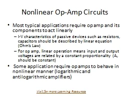
Most typical applications require op amp and its components to act linearly IV characteristics of passive devices such as resistors capacitors should be described by linear equation Ohms Law ID: 639751
Download Presentation The PPT/PDF document "Nonlinear Op-Amp Circuits" is the property of its rightful owner. Permission is granted to download and print the materials on this web site for personal, non-commercial use only, and to display it on your personal computer provided you do not modify the materials and that you retain all copyright notices contained in the materials. By downloading content from our website, you accept the terms of this agreement.


Slide1
Nonlinear Op-Amp Circuits
Most typical applications require op amp and its components to act linearlyI-V characteristics of passive devices such as resistors, capacitors should be described by linear equation (Ohm’s Law)For op amp, linear operation means input and output voltages are related by a constant proportionality (Av should be constant) Some application require op amps to behave in nonlinear manner (logarithmic and antilogarithmic amplifiers)
Visit for more Learning ResourcesSlide2
Logarithmic Amplifier
Output voltage is proportional to the logarithm of input voltageA device that behaves nonlinearly (logarithmically) should be used to control gain of op ampSemiconductor diodeForward transfer characteristics of silicon diodes are closely described by Shockley’s equationIF =
I
s
e
(V
F
/
η
V
T
)
I
s
is
diode saturation (leakage) current
e is base of natural logarithms (e = 2.71828)
V
F
is forward voltage drop across diode
V
T
is thermal equivalent voltage for diode (26 mV at 20°C)
η
is emission coefficient or ideality factor (2 for currents of same magnitude as I
S
to 1 for higher values of I
F
)Slide3
Basic Log Amp operation
D1
-
+
V
in
V
o
R
L
R
1
I
F
I
1
I
1
= V
in
/R
1
I
F
= - I
1
I
F
= - V
in
/R
1
V
0
= -V
F
= -
η
V
T
ln
(I
F
/I
S
)
V
0
= -
ηVT ln[Vin/(R1IS)] rD = 26 mV / IF IF < 1 mA (log amps)
At higher current levels (I
F
> 1
mA
) diodes begin to
behave somewhat linearlySlide4
Logarithmic Amplifier
Linear graph: voltage gain is very high for low input voltages and very low for high input voltagesSemilogarithmic graph: straight line proves logarithmic nature of amplifier’s transfer characteristicTransfer characteristics of log amps are usually expressed in terms of slope of V0 versus Vin plot in
milivolts
per decode
η
affects slope of transfer curve; I
S
determines the y intercept
Operational Amplifiers and Linear Integrated Circuits: Theory and Applications
by Denton J. DaileySlide5
Additional Log Amp Variations
Often a transistor is used as logging element in log amp (transdiode configuration)Transistor logging elements allow operation of log amp over wider current ranges (greater dynamic range)
Q
1
-
+
V
in
V
o
= V
BE
R
L
R
1
I
E
I
1
I
C
I
C =
I
ES
e
(V
BE
/V
T
)
- I
ES
is emitter saturation current
- V
BE
is drop across base-emitter junctionSlide6
Antilogarithmic Amplifier
Output of an antilog amp is proportional to the antilog of the input voltagewith diode logging elementV0 = -RFI
S
e
(V
in
/V
T
)
With
transdiode
logging elementV0 = -RF
IESe(Vin
/VT) As with log amp, it is necessary to know saturation currents and to tightly control junction temperature Slide7
Antilogarithmic Amplifier
D1
-
+
V
in
V
o
R
L
R
1
I
F
I
1
Q
1
-
+
V
in
V
o
R
L
R
F
I
F
I
1
I
E
(
α
= 1) I
1
= I
C
= I
ESlide8
Logarithmic Amplifier Applications
Logarithmic amplifiers are used in several areasLog and antilog amps to form analog multipliersAnalog signal processingAnalog Multipliersln xy = ln x + ln yln (x/y) = ln x – ln ySlide9
Analog Multipliers
Operational Amplifiers and Linear Integrated Circuits: Theory and Applications by Denton J. Dailey
D
1
-
+
-
+
R
L
V
o
-
+
-
+
R
R
R
R
V
y
V
x
R
R
D
2
D
3
One-quadrant multiplier: inputs must both be of same polaritySlide10
Analog Multipliers
Operational Amplifiers and Linear Integrated Circuits: Theory and Applications by Denton J. Dailey
Four quadrants of operation
General symbol
Two-quadrant multiplier: one input should have positive voltages, other input could have positive or negative voltages
Four-quadrant multiplier: any combinations of polarities on their inputsSlide11
Analog Multipliers
Operational Amplifiers and Linear Integrated Circuits: Theory and Applications by Denton J. Dailey
Implementation of mathematical operations
Squaring Circuit
Square root CircuitSlide12
Signal Processing
Many transducers produce output voltages that vary nonlinearly with physical quantity being measured (thermistor)Often It is desirable to linearize outputs of such devices; logarithmic amps and analog multipliers can be used for such purposesLinearization of a signal using circuit with complementary transfer characteristicsSlide13
Pressure Transmitter
Operational Amplifiers and Linear Integrated Circuits: Theory and Applications by Denton J. Dailey
Pressure transmitter produces an output voltage proportional to
difference in pressure between two sides of a strain gage sensor Slide14
Pressure Transmitter
A venturi is used to create pressure differential across strain gageOutput of transmitter is proportional to pressure differentialFluid flow through pipe is proportional to square root of pressure differential detected by strain gageIf output of transmitter is processed through a square root amplifier, an output directly proportional to flow rate is obtainedSlide15
Precision Rectifiers
Op amps can be used to form nearly ideal rectifiers (convert ac to dc)Idea is to use negative feedback to make op amp behave like a rectifier with near-zero barrier potential and with linear I/O characteristicTransconductance curves for typical silicon diode and an ideal diodeSlide16
Precision Half-Wave Rectifier
D1
-
+
V
in
V
o
R
L
R
1
I
2
I
1
R
F
D
2
I
2
I
2
V
x
Solid arrows represent current flow for positive half-cycles of V
in
and dashed arrows represent current flow for negative half-cyclesSlide17
Precision Half-Wave Rectifier
Operational Amplifiers and Linear Integrated Circuits: Theory and Applications by Denton J. Dailey
If signal source is going positive, output of op amp begins to go negative, forward biasing D
1
Since D
1
is forward biased, output of op amp
V
x
will reach a maximum level of ~ -0.7V regardless of how far positive V
in
goes
This is insufficient to appreciably forward bias D2, and V
0 remains at 0VOn negative-going half-cycles, D1 is reverse-biased and D
2 is forward biasedNegative feedback reduces barrier potential of D2 to 0.7V/A
OL (~ = 0)Gain of circuit to negative-going portions of Vin is given by A
V = -RF/R1Slide18
Precision Full-Wave Rectifier
D1
-
+
V
in
R
2
R
1
I
2
I
1
-
+
V
o
R
L
R
5
D
2
R
3
I
2
U
1
U
2
V
A
V
B
R
4
Solid arrows represent current flow for positive half-cycles of V
in
and dashed arrows represent current flow for negative half-cyclesSlide19
Precision Full-Wave Rectifier
Positive half-cycle causes D1 to become forward-biased, while reverse-biasing D2VB = 0 V VA = -Vin
R
2
/R
1
Output of U
2
is V
0
= -V
A R5/R4 = Vin
(R2R5/R1
R4)Negative half-cycle causes U1
output positive, forward-biasing D2 and reverse-biasing D1V
A = 0 V VB = -V
in R3/R1Output of U2 (noninverting configuration) is
V0
= VB [1+ (R5/R4
)]= - Vin [(R3/R1
)+(R3R5/R1
R4)if R3
= R1/2, both half-cycles will receive equal gainSlide20
Precision Rectifiers
Useful when signal to be rectified is very low in amplitude and where good linearity is neededFrequency and power handling limitations of op amps limit the use of precision rectifiers to low-power applications (few hundred kHz)Precision full-wave rectifier is often referred to as absolute magnitude circuitSlide21
ACTIVE FILTERSSlide22
Active Filters
Op amps have wide applications in design of active filtersFilter is a circuit designed to pass frequencies within a specific range, while rejecting all frequencies that fall outside this rangeAnother class of filters are designed to produce an output that is delayed in time or shifted in phase with respect to filter’s inputPassive filters: constructed using only passive components (resistors, capacitors, inductors)Active filters: characteristics are augmented using one or more amplifiers; constructed using op amps, resistors, and capacitors onlyAllow many filter parameters to be adjusted continuously and at will Slide23
Filter Fundamentals
Five basic types of filtersLow-pass (LP)High-pass (HP)Bandpass (BP)Bandstop (notch or band-reject)All-pass (or time-delay)Slide24
Response Curves
ω is in rad/sl H(jω) l denotes frequency-dependent voltage gain of filter
Complex filter response is given by
H(j
ω
) = l H(j
ω
) l <
θ
(j
ω
)If signal frequencies are expressed in Hz, filter response is expressed as l H(jf) l
Operational Amplifiers and Linear Integrated Circuits: Theory and Applications
by Denton J. DaileySlide25
Filter Terminology
Filter passband: range of frequencies a filter will allow to pass, either amplified or relatively unattenuatedAll other frequencies are considered to fall into filter’s stop band(s)Frequency at which gain of filter drops by 3.01 dB from that of passband determines where stop band begins; this frequency is called corner frequency (
f
c
)
Response of filter is down by 3 dB at corner frequency (3 dB decrease in voltage gain translates to a reduction of 50% in power delivered to load driven by filter)
f
c
is often called half-power pointSlide26
Filter Terminology
Decibel voltage gain is actually intended to be logarithmic representation of power gainPower gain is related to decibel voltage gain asAP = 10 log (P0/Pin)P
0
= (V
0
2
/Z
L
) and P
in
= (V
in2/Zin) A
P = 10 log [(V02/Z
L) /(Vin2/Z
in)]AP = 10 log (V0
2Zin /Vin
2ZL)]If ZL = Zin, A
P = 10 log (V0
2/Vin2) = 10 log (V0
/Vin)2A
P = 20 log (V0/Vin) = 20 log A
vWhen input impedance of filter equals impedance of load being driven by filter, power gain is dependent on voltage gain of circuit onlySlide27
Filter Terminology
Since we are working with voltage ratios, gain is expressed as voltage gain in dBl H(jω) ldB = 20 log (V0/Vin) = 20 log A
V
Once frequency is well into stop band, rate of increase of attenuation is constant (dB/decade
rolloff
)
Ultimate
rolloff
rate of a filter is determined by order of that filter
1
st
order filter: rolloff of -20 dB/decade2
nd order filter: rolloff of -40 dB/decadeGeneral formula for rolloff
= -20n dB/decade (n is the order of filter)Octave is a twofold increase or decrease in frequencyRolloff = -6n dB/octave (n is order of filter)Slide28
Filter Terminology
Transition region: region between relatively flat portion of passband and region of constant rolloff in stop bandGive two filter of same order, if one has a greater initial increase in attenuation in transition region, that filter will have a greater attenuation at any given frequency in stop bandDamping coefficient (α): parameter that has great effect on shape of LP or HP filter response in
passband
, stop band, and transition region (0 to 2)
Filters with lower
α
tend to exhibit peaking in
passband
(and
stopband
) and more rapid and radically varying transition-region response attenuation
Filters with higher α tend to pass through transition region more smoothly and do not exhibit peaking in
passband and stopband Slide29
LP Filter Response
Operational Amplifiers and Linear Integrated Circuits: Theory and Applications by Denton J. DaileySlide30
Filter Terminology
HP and LP filters have single corner frequencyBP and bandstop filters have two corner frequencies (fL and fU) and a third frequency labeled as f0
(center frequency)
Center frequency is geometric mean of
f
L
and
f
U
Due to log f scale, f
0 appears centered between fL and
fU f0
= sqrt (fLf
U)Bandwidth of BP or bandstop filter is
BW = fU – fL
Also, Q = f0 / BW (BP or bandstop filters)BP filter with high Q will pass a relatively narrow range of frequencies, while a BP filter with lower Q will pass a wider range of frequencies
BP filters will exhibit constant ultimate rolloff rate determined by order of the filterSlide31
Basic Filter Theory Review
Simplest filters are 1st order LP and HP RC sectionsPassband gain slightly less than unityAssuming neglegible loading, amplitude response (voltage gain) of LP section isH(jω) = (jXC) / (R + jX
C
)
H(j
ω
) = X
C
/sqrt(R
2
+X
C2) <-tan-1 (R/XC)
Corner frequency fc for 1st order LP or HP RC section is found by making R = X
C and solving for frequency R = XC = 1/(2
πfC) 1/fC = 2π
RC fC = 1/(2πRC)
Gain (in dB) and phase response of 1st order LP H(jf) dB = 20 log [1/{sqrt(1+(f/fc)2}] <-tan
-1 (f/fC)
Gain (in dB) and phase response of 1st order HP H(jf) dB = 20 log [1/{sqrt(1+(f
c/f)2}] <tan-1 (f
C/f)
Operational Amplifiers and Linear Integrated Circuits: Theory and Applications
by Denton J. Dailey
For more detail contact us