
TINA TI is a trademark of Texas Instruments WEBENCH is a registered trademark of Texas Instruments SLAU508 June 2013 Revised June 2013 Analog Pulse Width Modulation Copyright 2013 Texas Instruments Incorporated John Caldwell TI Precision Designs V ID: 22182
Download Pdf The PPT/PDF document "An IMPORTANT NOTICE at the end of this T..." is the property of its rightful owner. Permission is granted to download and print the materials on this web site for personal, non-commercial use only, and to display it on your personal computer provided you do not modify the materials and that you retain all copyright notices contained in the materials. By downloading content from our website, you accept the terms of this agreement.


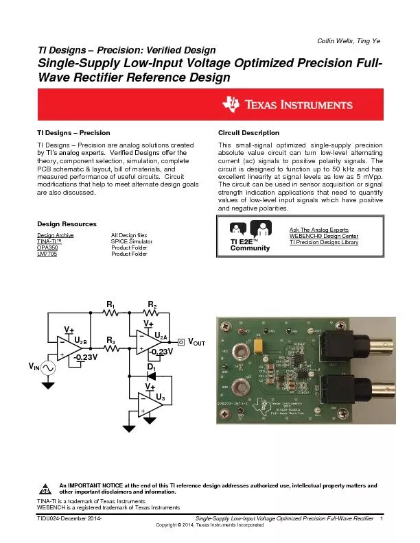
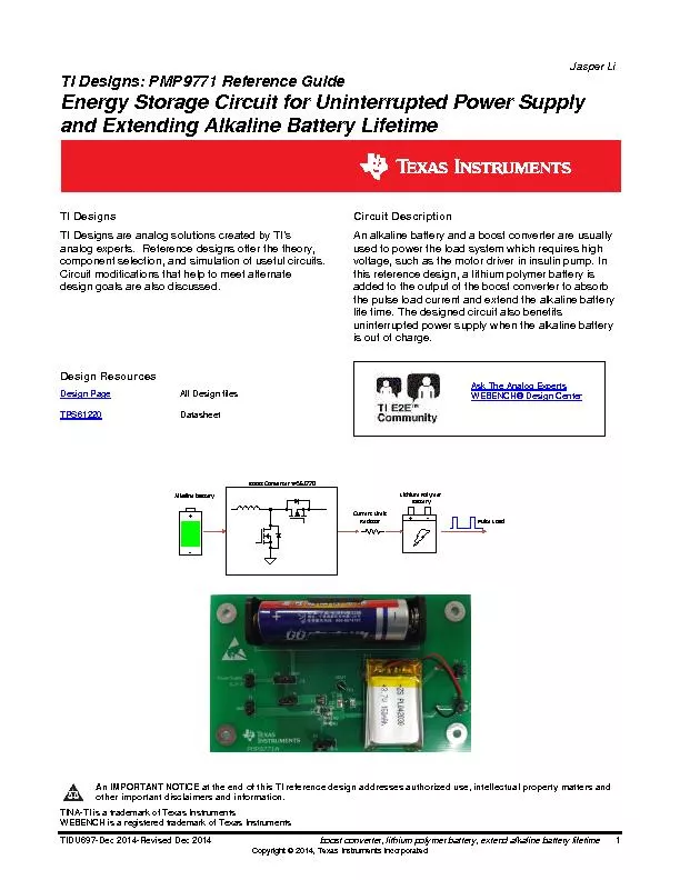


IMPORTANTNOTICEFORTIREFERENCEDESIGNS TexasInstrumentsIncorporated("TI")referencedesignsaresolelyintendedtoassistdesigners(Buyers)whoaredevelopingsystemsthat incorporateTIsemiconductorproducts(alsoreferredtohereinascomponents).BuyerunderstandsandagreesthatBuyerremains responsibleforusingitsindependentanalysis,evaluationandjudgmentindesigningBuyerssystemsandproducts. TIreferencedesignshavebeencreatedusingstandardlaboratoryconditionsandengineeringpractices.TIhasnotconductedany testingotherthanthatspecificallydescribedinthepublisheddocumentationforaparticularreferencedesign.TImaymake corrections,enhancements,improvementsandotherchangestoitsreferencedesigns. BuyersareauthorizedtouseTIreferencedesignswiththeTIcomponent(s)identifiedineachparticularreferencedesignandtomodifythe referencedesigninthedevelopmentoftheirendproducts.HOWEVER,NOOTHERLICENSE,EXPRESSORIMPLIED,BYESTOPPEL OROTHERWISETOANYOTHERTIINTELLECTUALPROPERTYRIGHT,ANDNOLICENSETOANYTHIRDPARTYTECHNOLOGY ORINTELLECTUALPROPERTYRIGHT,ISGRANTEDHEREIN,includingbutnotlimitedtoanypatentright,copyright,maskworkright, orotherintellectualpropertyrightrelatingtoanycombination,machine,orprocessinwhichTIcomponentsorservicesareused. InformationpublishedbyTIregardingthird-partyproductsorservicesdoesnotconstitutealicensetousesuchproductsorservices,ora warrantyorendorsementthereof.Useofsuchinformationmayrequirealicensefromathirdpartyunderthepatentsorotherintellectual propertyofthethirdparty,oralicensefromTIunderthepatentsorotherintellectualpropertyofTI. TIREFERENCEDESIGNSAREPROVIDED"ASIS".TIMAKESNOWARRANTIESORREPRESENTATIONSWITHREGARDTOTHE REFERENCEDESIGNSORUSEOFTHEREFERENCEDESIGNS,EXPRESS,IMPLIEDORSTATUTORY,INCLUDINGACCURACYOR COMPLETENESS.TIDISCLAIMSANYWARRANTYOFTITLEANDANYIMPLIEDWARRANTIESOFMERCHANTABILITY,FITNESS FORAPARTICULARPURPOSE,QUIETENJOYMENT,QUIETPOSSESSION,ANDNON-INFRINGEMENTOFANYTHIRDPARTY INTELLECTUALPROPERTYRIGHTSWITHREGARDTOTIREFERENCEDESIGNSORUSETHEREOF.TISHALLNOTBELIABLE FORANDSHALLNOTDEFENDORINDEMNIFYBUYERSAGAINSTANYTHIRDPARTYINFRINGEMENTCLAIMTHATRELATESTO ORISBASEDONACOMBINATIONOFCOMPONENTSPROVIDEDINATIREFERENCEDESIGN.INNOEVENTSHALLTIBE LIABLEFORANYACTUAL,SPECIAL,INCIDENTAL,CONSEQUENTIALORINDIRECTDAMAGES,HOWEVERCAUSED,ONANY THEORYOFLIABILITYANDWHETHERORNOTTIHASBEENADVISEDOFTHEPOSSIBILITYOFSUCHDAMAGES,ARISINGIN ANYWAYOUTOFTIREFERENCEDESIGNSORBUYERSUSEOFTIREFERENCEDESIGNS. TIreservestherighttomakecorrections,enhancements,improvementsandotherchangestoitssemiconductorproductsandservicesper JESD46,latestissue,andtodiscontinueanyproductorserviceperJESD48,latestissue.Buyersshouldobtainthelatestrelevant informationbeforeplacingordersandshouldverifythatsuchinformationiscurrentandcomplete.Allsemiconductorproductsaresold subjecttoTIstermsandconditionsofsalesuppliedatthetimeoforderacknowledgment. TIwarrantsperformanceofitscomponentstothespecificationsapplicableatthetimeofsale,inaccordancewiththewarrantyinTIsterms andconditionsofsaleofsemiconductorproducts.TestingandotherqualitycontroltechniquesforTIcomponentsareusedtotheextentTI deemsnecessarytosupportthiswarranty.Exceptwheremandatedbyapplicablelaw,testingofallparametersofeachcomponentisnot necessarilyperformed. TIassumesnoliabilityforapplicationsassistanceorthedesignofBuyersproducts.Buyersareresponsiblefortheirproductsand applicationsusingTIcomponents.TominimizetherisksassociatedwithBuyersproductsandapplications,Buyersshouldprovide adequatedesignandoperatingsafeguards. ReproductionofsignificantportionsofTIinformationinTIdatabooks,datasheetsorreferencedesignsispermissibleonlyifreproductionis withoutalterationandisaccompaniedbyallassociatedwarranties,conditions,limitations,andnotices.TIisnotresponsibleorliablefor suchaltereddocumentation.Informationofthirdpartiesmaybesubjecttoadditionalrestrictions. Buyeracknowledgesandagreesthatitissolelyresponsibleforcompliancewithalllegal,regulatoryandsafety-relatedrequirements concerningitsproducts,andanyuseofTIcomponentsinitsapplications,notwithstandinganyapplications-relatedinformationorsupport thatmaybeprovidedbyTI.Buyerrepresentsandagreesthatithasallthenecessaryexpertisetocreateandimplementsafeguardsthat anticipatedangerousfailures,monitorfailuresandtheirconsequences,lessenthelikelihoodofdangerousfailuresandtakeappropriate remedialactions.BuyerwillfullyindemnifyTIanditsrepresentativesagainstanydamagesarisingoutoftheuseofanyTIcomponentsin Buyerssafety-criticalapplications. Insomecases,TIcomponentsmaybepromotedspecificallytofacilitatesafety-relatedapplications.Withsuchcomponents,TIsgoalisto helpenablecustomerstodesignandcreatetheirownend-productsolutionsthatmeetapplicablefunctionalsafetystandardsand requirements.Nonetheless,suchcomponentsaresubjecttotheseterms. NoTIcomponentsareauthorizedforuseinFDAClassIII(orsimilarlife-criticalmedicalequipment)unlessauthorizedofficersoftheparties haveexecutedanagreementspecificallygoverningsuchuse. OnlythoseTIcomponentsthatTIhasspecificallydesignatedasmilitarygradeorenhancedplasticaredesignedandintendedforusein military/aerospaceapplicationsorenvironments.BuyeracknowledgesandagreesthatanymilitaryoraerospaceuseofTIcomponentsthat havenotbeensodesignatedissolelyatBuyer'srisk,andBuyerissolelyresponsibleforcompliancewithalllegalandregulatory requirementsinconnectionwithsuchuse. TIhasspecificallydesignatedcertaincomponentsasmeetingISO/TS16949requirements,mainlyforautomotiveuse.Inanycaseofuseof non-designatedproducts,TIwillnotberesponsibleforanyfailuretomeetISO/TS16949. MailingAddress:TexasInstruments,PostOfficeBox655303,Dallas,Texas75265 Copyright©2013,TexasInstrumentsIncorporated An IMPORTANT NOTICE at the end of this TI reference design addresses authorized use, intellectual property matters and other important disclaimers and information. TINA - TI is a trademark of Texas Instruments WEBENCH is a registered trademark of Texas Instruments SLAU508 - June 2013 - Revised June 2013 Analog Pulse Width Modulation 1 Copyright © 2013, Texas Instruments Incorporated John Caldwell TI Precision Designs : Verified Design Analog Pulse Width Modulation TI Precision Designs Circuit Description TI Precision Designs are analog solutions created by TIâs analog experts. Verified Designs offer the theory, component selection, simulation , complete PCB schematic & layout, bill of materials, and measured performance of useful circuits. Circuit modifications that help to meet alternate design goals are also discussed. This circuit utilizes a triangle wave generator and comparat or to generate a pulse - width - modulated (PWM) waveform with a duty cycle that is inversely proportional to the input voltage. An op amp and comparator generate a triangular waveform which is passed to the inverting input of a second comparator. By passing t he input voltage to the non - inverting comparator input, a PWM waveform is produced. Negative feedback of the PWM waveform to an error amplifier is utilized to ensure high accur acy and linearity of the output Design Resources Design Archive All Design files TINA - T I⢠SPICE Simulator OPA2365 Product Folder TLV3502 Product Folder REF3325 Product Folder Ask The Analog Experts WEBENCH® Design Center TI Precision Designs Library www.ti.com 2 Analog Pulse Width Modulation SLAU508 - June 2013 - Revised June 2013 Copyright © 2013, Texas Instruments Incorporated 1 Design Summary The design requirements are as follows: ï· Supply voltage: 5 Vdc ï· Input voltage: - 2 V to +2 V , dc coupled ï· Output: 5 V, 500 kHz PWM ï· Ideal transfer function: à ͳ à Í´ Í· V The design goals and performance are summarized in Table 1 . Table 1 : Design goals and performance summary. Goals Simulated Measured THD (1 Vrms, 1 kHz) 0.1% NA 0.009% Offset Error (%) 5% 2.324% 0.108% Gain Error (%) 5% 4.5% 0.22% Figure 1 depicts the operation of the circuit. An input waveform is converted to a 5 Vp, 500 kHz PWM waveform. The duty cycle of the waveform is inverted from the input signal. Figure 1 : Actual PWM output (top) for a 20 kHz, 1.5 Vp input sine wave (bottom). www.ti.com SLAU508 - June 2013 - Revised June 2013 Analog Pulse Width Modulation 3 Copyright © 2013, Texas Instruments Incorporated 2 Theory of Operation Lowpass filtering a PWM waveform produces an output voltage that follows the function: à à à ( 1 ) Where V O is the averaged output voltage, δ is the duty cycle of the PWM waveform, and V PWM is its amplitude. For example, a 5 V PWM waveform with a duty cycle of 75% would produce an output voltage of 3.75 V when lowpass filtered. This concept is extremely useful in many applications such as Class - D audio amplifiers, switching power supplies, optical transmission, and conveying analog information through digital isolation. This circuitâs operation can be bet ter understood by breaking it into three parts: a comparator, an error amplifier, and a triangle wave generator. Figure 2 : Complete circuit schematic with functional portions highlighted. www.ti.com 4 Analog Pulse Width Modulation SLAU508 - June 2013 - Revised June 2013 Copyright © 2013, Texas Instruments Incorporated 2.1 Output Comparator Function The operation of the output comparator (one half of dual comparator U2) is b est understood graphically. Figure 3 depicts the two inputs to the comparator ( top, tria ngle and sine wave ) as well as the output ( bottom). The triangle wave is applied to the negative input of the comparator. The sinusoid represents a signal applied to the positive input of the comparator. Notice that when the value of the triangle wave is greater than the value of the input signal, the output of the comparator is low. Conversely, when the value of the input signal is great er than that of the triangle wave, the output of the comparator is high. This simple method produces an output square wave with a duty cycle that varies depending on an input voltage. Figure 3 : The output of a comparator (green) with a triangle wave applied to its negative input (blue) and a sine wave applied to its positive input (red). A.1 Error Amplifier Design The error amplifier, composed of one half of the dual op amp U1, serves two purposes. First, the error amplifier accommod ates feedback of the output PWM waveform in order to correct for any errors in the output voltage introduced by the comparator. Second, it adds a dc offset to the input voltage so that negative input voltages can be accommodated by the circuit. Figure 4 : The error amplifier and output comparator with calculated component values. www.ti.com SLAU508 - June 2013 - Revised June 2013 Analog Pulse Width Modulation 5 Copyright © 2013, Texas Instruments Incorporated Many PWM circuits operate without the comparator included in the feedback loop of an amplifier. For these circuits, the output duty cycle is a function of the amplitude of the triangle wave (V TRI ) and amplitude of the input signal (V IN ) . The average output voltage (V O ) depends on the amplitude of the PWM waveform (V PWM ) which is typically determined by the supply voltages of the comparator. à à à àà à Í´ àà à à ( 2 ) Because the supply voltage of the comparator directly impacts the output voltage, PWM circuits without feedback have no power supply rejection. In this TI Design, the error amplifier acts as an inverting amplifier to the input signal, shown as a dc - coupled source V IN . By including the comparator inside the feedback loop of the error amplifier, and adding integration capacitor C1, the error amplifier now directly controls the average output voltage. à ସ ଷ à à ( 3 ) T he pow er supply voltage of the comparator no longer affects the average output voltage, showing the benefits of negative feedback on power supply rejection. Using values of 10kOhms for R4 and R3 produces the desired signal gain of - 1. The value of capacitor C1 m ust be chosen to limit the bandwidth of the error amplifier to below the switching frequency in order to ensure stability of the system. This will also limit the signal bandwidth, so a value must be chosen which does not interfere with the desired signal b andwidth. C1 creates a pole in the frequency response at: ͳ Í´ ସ ଵ ( 4 ) A value of 100 pF for C1 creates a pole in the frequency response at 159 kHz and causes negligible attenuation of the signal within the audio frequency range (20 Hz to 20 kHz).An offset is added to the signal (VREF) such that input signals that extend below ground may be accommodated. Because the offset voltage, provided by 2.5 V reference U3, is applied to the non - inverting input of amplifier U1A, it is amplified according to the equation: à ͳ ସ ଷ à ( 5 ) Resistors R1 and R2 are necessary to divide the reference voltage by two, in order to compensate for the non - inverting gain of two applied by the error amplifier. Thus, the DC offset at the output of U1A is: à ͳ ସ ଷ ଶ ଵ ଶ à ͳ ͳͲ ͳͲ ͳͲ ͳͲ ͳͲ Í´ Í· Í´ Í· ( 6 ) AC coupling the input signal through a capacitor will reduce the non - inverting gain to unity. In this case, resistor R 2 can be removed from the circuit. Capacitor C2 is included at the non - inverting input to filter any interference which may be introduced to the non - inverting input. 2.2 Triangle Wave Generator The other halves of the dual op amp and comparator form the basis for the triangle wave generator. The operation of this circuit is well described in reference 1 and this document draws on that publication for several design equations. www.ti.com 6 Analog Pulse Width Modulation SLAU508 - June 2013 - Revised June 2013 Copyright © 2013, Texas Instruments Incorporated Figure 5 : Triangle wave generator circuit with calculated component values. The op amp is configured as an integrator and its output increases linearly when the comparator output is low. Conversely, the output decreases linearly when the comparator output is high. The comparator output switches w hen the voltage at its non - inverting input passes through the reference voltage, which is 2.5V in this circuit. Because this circuit is designed to be powered from a single 5V supply, a 2.5V offset was added to the triangle wave such that it is centered at the mid - supply point for all components in the circuit. The amplitude of the triangle wave is defined by the equation: àà ହ ଺ ଵ ( 7 ) In this equation, V 1 is the comparator output voltage above or below the reference voltage. For example, in our system the comparator output will be either 5V or 0V. Because this circuit employs a 2.5V reference, V 1 is equal to 2.5V. Most PWM systems do not allow for 0% or 10 0% modulation because the output would be DC and may damage other components in the signal path. Therefore, the amplitude of the triangle wave must be chosen such that it is greater than the maximum expected input voltage. Choosing an amplitude of 2.1V wil l allow for the required input range of - 2V to +2V. By selecting a value of 10kOhms for R6, the value of R5 can be calculated: ହ àà ଺ ଵ Í´ ͳ ͳͲ Í´ Í· ͺͶʹͳ Ͳͷ ͺ Ͷͷ ( 8 ) A value of 8.45 kOhms is the closest 1% value to the calculated value. Low resistor values in the triangle wave generator circuit can cause excess current to be drawn from the op amp output. This may have the effect of distorting the triangular waveform shape. Although higher triangle wave ampl itudes would allow for larger input voltages, we are limited by the output voltage range of the op amp. The oscillation frequency of the triangle wave generator is calculated from this equation: à ଺ Ͷ ଻ ହ ଷ ( 9 ) Selecting a value of 100 pF for C 3 allows us to calculate R 7 for a 500 kHz triangle wave: www.ti.com SLAU508 - June 2013 - Revised June 2013 Analog Pulse Width Modulation 7 Copyright © 2013, Texas Instruments Incorporated ଻ ଺ Ͷ à ହ ଷ ͳͲ Ͷ ͷͲͲ ͺ Ͷͷ ͳͲͲ ͷͻͳ͹ ͳ͸ Í· ͻͲ ( 10 ) 3 Component Selection 3.1 Amplifier Selection In order to use a dual operation al amplifier for this circuit, one must consider the demands of both the error amplifier and the triangle wave generator portions of the circuit. Examining at the triangle wave generator portion the slew rate and bandwidth of the op amp must be considered. The slew rate of the linear portion of the triangle wave is: à Ͷ àà àà Ͷ Í´ ͳ ͷͲͲ Ͷ Í´ ( 11 ) An op amp with a slew rate much greater than 4.2 V/ μ s must be used in this circuit in order to prevent distortion of the triangle wave. A triangle wave is an infinite summation of sinusoids which are odd - ordered integer multiples of the fundamental. Using a rule of thumb that 10 harmonics are the minimum necessary to produce a triangular wave, we can determine that the bandw idth of the op amp must be greater than 19 times the triangle wave frequency. This is because the 10 th harmonic of a triangle wave has a frequency 19 times the fundamental. ͳͻ àà ͳͻ ͷͲͲ Í» Í· ( 12 ) The op amp is confi gured as an integrator in the triangle wave circuit. In this configuration, the input bias current of the op amp can contribute error to the triangle wave shape by delivering or removing extra charge from the integration capacitor C3. For this reason, a FE T type op amp is recommended because the extremely low bias currents of these amplifiers will not add appreciable error to the triangle wave shape. Finally, the output of the op amp must be able to produce voltages near the supply voltages. The triangle wa ve in this circuit has an amplitude of 2.1V and an offset of 2.5V giving it maximum and minimum voltag es of 4.6V and .4V respectively. T he op amp must be able to output voltages less than 400mV from either supply rail if it is powered from a single 5V supp ly. The additional demands placed on the dual op amp are from the error amplifier portion of the circuit. For DC applications, the op ampâs input offset voltage and offset voltage drift may introduce inaccuracies in the output waveform. More commonly howe ver, DC inaccuracy is dominated by the tolerance of resistors R2, R3, R4, and R5. The OPA2365 chosen for this circuit is a FET - input dual op amp that has a gain bandwidth product of 50 MHz and a typical slew rate of 25 V/ μ s. The maximum offset of the OPA23 65 is 200 μ V with a maximum offset drift of 1 μ V/ ° C. These specifications make the OPA2365 an excellent candidate for both the error amplifier and triangle wave portions of the circuit. 3.2 Comparator Selection The comparator used must have a push - pull output topology. Many comparators have an open collector or open drain output topology. Although an open drain output allows the output voltage to be rapidly pulled low, the output voltage can only be pulled high through an external resistor. Low value res istors allow for fast rise times on the output but cause excess power dissipation while the output is pulled low. In the triangle wave circuit, a comparator with an open drain output would also have different rise and fall times at its output, distorting t he triangle wave. For proper operation of the triangle wave generator and stability of the control loop the propagation delay of the comparator must be much less than the period of the PWM waveform. à à ( 13 ) Keeping the c omparator propagation delay less than 1/10 th the period of the PWM waveform is a good design goal. The phase delay introduced by the comparator can be calculated using the equation: www.ti.com 8 Analog Pulse Width Modulation SLAU508 - June 2013 - Revised June 2013 Copyright © 2013, Texas Instruments Incorporated ͵͸Ͳ ( 14 ) Because the propagation delay of the comparator must be much less than the period of the PWM waveform, the comparator will not introduce significant phase delay into the feedback loop until frequencies well above the switching frequency. This is why choosing a pole frequency for the e rror amplifier less than the switching frequency allows for stable operation. The TLV3502 used here has a push - pull output and a typical propagation delay of 4.5 ns making it a good candidate for systems with high PWM frequencies. 3.3 Passive Component Selecti on Resistors The tolerance of resistors R1, R2, R3, and R4 is directly responsible for the output offset error and gain error. For the purposes of this document, 1% resistors were used because they were readily available however improvements in the dc perf ormance and gain accuracy of the circuit can be achieved from using resistors with tighter tolerances. Capacitors The type of capacitor used for C1 and C3 can have a direct effect on the performance of this circuit. Because both of these capacitors can hav e a substantial voltage across them, the voltage coefficient of high - k ceramic capacitors can introduce non - linearity in both the error amplifier and triangle wave generator. Ceramic capacitors with an NP0/C0G dielectric were used for these two capacitors. All other capacitors were of the X7R typ e. www.ti.com SLAU508 - June 2013 - Revised June 2013 Analog Pulse Width Modulation 9 Copyright © 2013, Texas Instruments Incorporated 4 Simulation Because this circuitâs operation depends on rapid changes in output voltages as well as an oscillator circuit, it is best to simulate the design in separate parts to confirm functionality and avoid convergence issues in SPICE simulators. For this reason, the error amplifier and comparator were simulated separately from the triangle wave generator. 4.1 Triangle Wave Generator The Tina - TI⢠schematic used to simulate the triangle wave generator portion of the circuit is shown in Figure 6 . It includes component values that were calculated in the âTheory of Operationâ portion of this document. Figure 6 : Tina - TI ⢠simulation schematic of the triangle wave generator. Transient Analysis A transient analysis can be used to confirm that the amplitude and frequency of the triangle waveform are close to the intended values. www.ti.com 10 Analog Pulse Width Modulation SLAU508 - June 2013 - Revised June 2013 Copyright © 2013, Texas Instruments Incorporated Figure 7 : Transient analysis results displaying the output voltage of the triangle wave generator Table 2 : Comparison of the design goals and simulation results for the triangle wave generator Design Goal Simulat ion Frequency 500 kHz 483.6 kHz Amplitude 2.1 V 2.21 V 4.2 Error Amplifier and Comparator In order to simulate the functionality of the error amplifier and comparator, the triangle wave generator portion of the circuit was replaced with a voltage controlled oscillator (VCO) block which outputs a 500 kHz triangle wave with a 2.5 V offset and 2.1 V amplitude. This allows for faster simulation times and also mitigates convergence issues. Figure 8 : Tina - TI ⢠simulation schematic of th e error amplifier and output comparator. www.ti.com SLAU508 - June 2013 - Revised June 2013 Analog Pulse Width Modulation 11 Copyright © 2013, Texas Instruments Incorporated Transient Analysis A transient analysis is used to ensure proper functionality of the circuit. As shown in Figure 9 , the output is a 500 kHz PWM waveform with a 5 V amplitude. Again, because the error amplifier is in an inverting configuration, the polarity of the output signal is inverted. Figure 9 : Transient analysis of the error amplifier and comparator showing the comparator output (top, red) and the input waveform (bottom, green). DC Transfer Characteristic Performing a dc transfer characteristic sweep shows that the av erage output voltage follows the desired transfer function if the circuit is built with ideal component values for R1 through R4. The voltage plotted in Figure 10 is measured at VPWM in the schematic in Figure 8 . Because this simulation is a dc transfer characteristic, the plotted voltage is the average value of the PWM waveform. Figure 10 : A DC transfer characteristic sweep showing the average output voltage of the circuit when built with ideal components . www.ti.com 12 Analog Pulse Width Modulation SLAU508 - June 2013 - Revised June 2013 Copyright © 2013, Texas Instruments Incorporated Performing a 100 - sweep Monte Carlo analysis of the circuit, using 1% tolerances for the resistors w ith a Gaussian distribution shows more realistic values for the output at different input voltages. Table 3 : Monte Carlo analysis results for different input voltages. Input Designed Output Simulation Output (Min) Simulation Output (Max) Average Standard Deviation 0V 2.5 V 2.4419 V 2.549304 V 2.501631 V 0.0235407 V - 2V 4.5 V 4.367954 V 4.618445 V 4.500606 V 0.0468972 V +2V 0.5 V 0.436538 V 0.549543 V 0.502656 V 0.02322183 V These numbers reveal a potential gain error of +/ - 4.5% and a potential offset of 58.1mV or 2.324% error. Using resistors with tighter tolerances can greatly increase the DC accuracy of this circuit. 4.3 Simulated Results Summary Comparing the simulated results to the design goals shows that the design requirements will be met even when factoring in the component tolerances, as shown in the Monte Carlo analysis. Table 4 : Comparison of des ign goals and simulated results Goals Simulated THD (1Vrms, 1kHz) 0.1% NA Offset Error (%) 5% 2.324% Gain Error (%) 5% 4.5% www.ti.com SLAU508 - June 2013 - Revised June 2013 Analog Pulse Width Modulation 13 Copyright © 2013, Texas Instruments Incorporated 5 PCB Design The PCB schematic and Bill of Materials can be found in the appendix . 5.1 PCB Layout The fast edge rates of the output PWM signal can be capacitively coupled back into the signal path or reference voltage. The PCB layout for this TI design seeks to minimize trace lengths and loop areas, and separates the error amplifier portion of the circ uit from the triangle wave generator and PWM outputs. Jumper JP1 can be removed to accommodate ac coupling of the input signal. If this is desired, resistor R2 must be removed in order to maintain the proper dc offset at the output. Resistor R4 closes the error amplifier feedback loop around the comparator. However, R4 can be uninstalled and resistor R8 (on the bottom of the PCB) can be installed to close the error amplifier feedback loop excluding the comparator. Figure 11 : Top view of the PCB layout. www.ti.com 14 Analog Pulse Width Modulation SLAU508 - June 2013 - Revised June 2013 Copyright © 2013, Texas Instruments Incorporated 6 Verification & Measured Performance The output of the triangle wave generator circuit was examined to confirm that it met the designed specifications. The output of this circuit is shown in Figure 12 , the amplitude of the triangle wave was 2.087 V and the frequency was 477 kHz. These values were suitably close to the design values for the total system performance to meet t he design specifications. Figure 12 : Output of the triangle wave generator circuit Basic functionality of the circuit was confirmed by viewing the output PWM waveform on an oscilloscope and observing the change in duty cycle whe n an input signal is applied. Figure 13 : Pulse width modulated waveform (top) produced by an input 20 kHz, 1.5 Vp input sine wave (bottom) In order to recover the average output voltage V O from the PWM waveform, a lowpass filter must be placed at the output of the circuit. Figure 14 shows the passive 4 th - order Butterworth lowpass filter used to recover the average output voltage and facilitate the measurement of the dc transfer function and distortion performance of the circuit. www.ti.com SLAU508 - June 2013 - Revised June 2013 Analog Pulse Width Modulation 15 Copyright © 2013, Texas Instruments Incorporated Figure 14 : A 4th - order Butterworth lowpass filter used to measure the average output voltage of the PWM waveform Placing this filter on the output of the circuit, we can see that the average output voltage is indeed an inverted representation of the input signal. Figure 15 : Lowpass filtered output (top) shows proper reconstruction of the input signal with phase inverted. 6.1 Transfer Function The transfer function of the circuit was measured by varying the input voltage and measuring the voltage after the filter with a 6.5 digit voltmeter. The gain of the circuit was - 0.9 978 V/V which is a gain error of 0.22%. The offset of the circuit was measured at 2.4973 V , producing an offset error of 0.108%. Because the measured transfer function so closely follows the ideal transfer function for the circuit, the deviation between me asured and ideal was plotted separately. Figure 17 displays the total transfer function error which includes both offset and gain error. The worst cas e deviation from ideal occurs for a 2 V input which produced and output error of 0.32%. www.ti.com 16 Analog Pulse Width Modulation SLAU508 - June 2013 - Revised June 2013 Copyright © 2013, Texas Instruments Incorporated Figure 16 : The transfer function of the circuit measured by lowpass filtering the output waveform. Figure 17 : Total measured transfer function error. 0 0.5 1 1.5 2 2.5 3 3.5 4 4.5 5 - 2 - 1.5 - 1 - 0.5 0 0.5 1 1.5 2 Output Voltage Input Voltage (V) Measured Transfer Function 0.00% 0.05% 0.10% 0.15% 0.20% 0.25% 0.30% 0.35% - 2 - 1.5 - 1 - 0.5 0 0.5 1 1.5 2 Output Error (%) Input Voltage (VDC) Transfer Function Error www.ti.com SLAU508 - June 2013 - Revised June 2013 Analog Pulse Width Modulation 17 Copyright © 2013, Texas Instruments Incorporated 6.2 Total Harmonic Distortion and Noise Because PWM circuits are commonly used in audio applications, the total harmonic distortion and noise (THD+N) of the circuit was measured over the 20 Hz to 20 kHz frequency range for a 1 Vrms input signal. A 4 th - order passive Butterworth lowpass filter with a corner frequency of 40 kHz was added to the output of the circuit to recover the input signal. An audio analyzer configured with an AES17 40 kHz input filter was used to perform the measurements. The plot shows the THD+N for the circuit configured two ways. The red trace is the output THD+N when the feedback loop incorporates the output comparator (closed loop). The blue trace is the output THD +N when the feedback loop only includes the error amplifier (open loop). Figure 18 : Measured THD+N of the lowpass filtered PWM waveform. THD+N is greatly reduced by closing the error amplifier feedback loop around the comparato r (red). 6.3 Measured Result Summary The measured results of the circuit exceed the design goals by a large amount in every category. However, these results are for a single unit. If a large number of units were built, it is likely that some units would exhibi t the offset and gain error magnitudes shown in the Monte Carlo simulation. Table 5 : A comparison of the measured results to the design goals Goals Measured THD (1Vrms, 1kHz) 0.1% 0.009% Offset Error (%) 5% 0.108% Gain Error (%) 5% 0.22% 7 Modifications Several dual operational amplifiers meet the design requirements of wide bandwidth, high slew rate, low input offset voltage and low offset voltage drift. Selecting an alternative amplifier depends on the dominant performance goals of the project. For example, selecting an OPA2376 could potentially improve the DC accuracy of the circuit due to its improved offset and drift specifications. However, because this amplifier has a lower bandwidth and slew rate than the OPA2365, the PWM f requency would need to be reduced. One modification that may improve the performance of this system is to use separate single - channel amplifiers for the error amplifier and triangle wave generator. This would allow for both high DC precision and fast PWM f requencies, while reducing power consumption. 0.001 0.01 0.1 1 10 100 1000 10000 100000 THD+N (%) Frequency (Hz) Distortion of Filtered PWM Waveform Open Loop Closed Loop www.ti.com 18 Analog Pulse Width Modulation SLAU508 - June 2013 - Revised June 2013 Copyright © 2013, Texas Instruments Incorporated Table 6 : Several alternative amplifiers compared with the OPA2365 Amplifier Max Offset Voltage (uV) Max Offset Drift (uV/°C) Gain Bandwidth (MHz) Slew Rate (V/us) Supply Current (mA/ch) OPA2365 200 1 50 25 4.6 OPA2320 150 5 20 10 1.5 OPA2350 500 4 38 22 5.2 OPA2376 25 1 5.5 2 0.76 Because the dual comparator must have a push - pull output topology and an extremely low propagation delay, the number of alternative comparators is greatly limited. The TLV3202 is one alternative which offers reduced power supply consumption with a slightly slower propagation dely. It is important to note that the TLV3202 does not have a compatible pin out with the TLV3502 and will not work on the PCB layout presented herein. Table 7 : Comparison of TLV3202 and TLV3502 comparators Comp arator Supply Current (mA/ch) Propagation Delay (nS) TLV3502 3.2 4.5 TLV3202 0.04 40 8 About the Author John Caldwell is an applications engineer with Texas Instruments Precision Analog, supporting operational amplifiers and industrial linear devices. He specializes in precision circuit design for sensors, low - noise design and measurement, and electromagnet ic interference issues. He received his MSEE and BSEE from Virginia Tech with a research focus on biomedical electronics and instrumentation. Prior to joining TI in 2010, John worked at Danaher Motion and Ball Aerospace. 9 Acknowledgements & References 1. W.M . Leach, Introduction to Electroacoustics and Audio Amplifier Design: The Class - D Amplifier, Iowa: Kendall/Hunt Publishing Co., 2001. www.ti.com SLAU508 - June 2013 - Revised June 2013 Analog Pulse Width Modulation 19 Copyright © 2013, Texas Instruments Incorporated Appendix A. A.1 Electrical Schematic Figure A - 1: Electrical Schematic www.ti.com 20 Analog Pulse Width Modulation SLAU508 - June 2013 - Revised June 2013 Copyright © 2013, Texas Instruments Incorporated A.2 Bill of Materials Quantity Value Designator Description Manufacturer Manufacturer Part # Supplier Part # 2 100pF C1, C3 CAP, CERM, 100pF, 50V, +/ - 5%, C0G/NP0, 0603 AVX 06035A101JAT2A 478 - 1175 - 1 - ND 6 0.1uF C2, C5, C8, C9, C10, C11 CAP, CERM, 0.1uF, 16V, +/ - 5%, X7R, 0603 AVX 0603YC104JAT2A 478 - 3726 - 1 - ND 1 1uF C4 CAP, CERM, 1uF, 25V, +/ - 10%, X7R, 1206 Kemet C1206C105K3RACTU 399 - 1255 - 1 - ND 2 4.7uF C6, C7 CAP, CERM, 4.7uF, 16V, +/ - 10%, X5R, 1206 Kemet C1206C475K4PAC TU 4520506 2 J1, J2 Right Angle BNC Connector TE Connectivity 1 - 1634612 - 0 571 - 1 - 1634612 - 0 2 J3, J4 Standard Banana Jack, Uninsulated, 5.5mm Keystone 575 - 4 575 - 4K - ND 1 JP1 Two pin male header for jumper Samtec 87224 - 2 A26543 - ND 6 10.0k R1, R2, R3, R4, R6, R8 (DNI) RES, 10.0k ohm, 1%, 0.1W, 0603 Vishay - Dale CRCW060310K0FKEA 541 - 10.0KHCT - ND 1 8.45k R5 RES, 8.45k ohm, 1%, 0.1W, 0603 Vishay - Dale CRCW06038K45FKEA 541 - 8.45KHCT - ND 1 5.90k R7 RES, 5.90k ohm, 1%, 0.1W, 0603 Vishay - Dale CRCW06035K90FKEA 541 - 5.90KHCT - ND 1 U1 OPA2365 Dual Operational Amplifier Texas Instruments OPA2365AID 595 - OPA2365AID 1 U2 TLV3502 Dual Comparator Texas Instruments TLV3502AID 296 - 18301 - 5 - ND 1 U3 REF3325, 2.5V Low Power Voltage Reference Texas Instruments REF3325AIDCKT 296 - 22642 - 2 - ND