/


of deliverable chips in 65nm run M14 June 2016 MS42 Final design review of 65nm M30 October 2017 MS43 Test report of deliverable D41 ID: 791476
Download The PPT/PDF document "MS4.1 Architectural review" is the property of its rightful owner. Permission is granted to download and print the materials on this web site for personal, non-commercial use only, and to display it on your personal computer provided you do not modify the materials and that you retain all copyright notices contained in the materials. By downloading content from our website, you accept the terms of this agreement.
Slide1
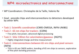
MS4.1 Architectural review of deliverable chips in 65nm run M14 (June 2016) MS4.2 Final design review of 65nm M30 (October 2017) MS4.3 Test report of deliverable D4.1 M46 (February 2019) MS4.4 Selection of SiGe foundry M14 MS4.5 Final design review of deliverable chips in SiGe run M30 MS4.6 Test report of deliverable D4.2 M46 MS4.7 Selection of TSV process M14 MS4.8 Final design review of deliverable D4.3 M30 MS4.9 Test report of deliverable D4.3 M46
AIDA WP4
milestones
Slide2WP4.3 : SiGe 130 nm microelectronics(CNRS-IPNL, CNRS-OMEGA, DESY, AGH-UST) Coordination: CNRS-OMEGA Select best SiGe 130/180 nm process for high speed/high dynamic range ASIC design to upgrade current SiGe 350 nm AMS process Deliver SPIROC3 SiPM readout for calorimeter readout of WP14 Deliver RPC high timing readout chip for WP13 Share expertise within SiGe HEP community Study for LHC run 2, ILC…
Slide3SiGe processes evalutatedST Micro SiGe 130 nmDesign kit installed at OMEGA mid 2015 and runningSimulations performed for ATLAS LAr calo upgradeSimulations for CMS HGCAL imaging calo and 50 ps timingSimulations for timing detectors e.g. ATLAS HGTDTower Jazz SiGe 130 nmAfter several requests, design kit never supplied
Slide4Testbenches for SiGeLow noise line terminating preamp for ATLAS LArG upgradeCurrent version uses bipolar transistors to achieve en=0.4 nV/√HzDynamic range up to 10 mA25/50 active termination over full dynamic rangeLow noise system on chip for CMSHGCALCharge and time measurementHigh speed LGAD or RPC readout1 GHz broadband amplifier
Slide5New preamp design for LArG08/03/16 ACES meeting
Super
common base preamp (low Zin) Low noise voltage sensitive preamp
Input Impedance
:
Noise
Better in CMOS than
SiGe
at
Ic
=10 mA because
of R
BB’ and parallel noise
50
25 R0500 100 GC1/C2=9 C1/C2=3 Noise 5 6Dynamic 2 mA with Rf=5k10 mA with Rf=1k
Slide6CE in SiGe 130nm and in TSMC 130 nmBroad Band amplifier CE configurationSame current (Ic=700 µA), same Rf=4K, vdd=1.2VHigher gain with SiGe but larger noise due to rbb’HGTD Electronics - Workshop April 20166CE 10pF TSMC 130 nmCE 10pF SiGe 130nmTrans size= 10CE 10pFSiGe 130nmTrans size= 20td=10ps Qin=Iin.td= 100µA.10ps=1fCout=3.7mV tr=220ps BWa=1.6 GHzrms=1.3 mV
S/N=2.8
σj
=220ps/2.8=78
ps
out=9.07mV
tr=140ps
BWa
=2.4 GHz
rms
=4 mV
S/N=2.25
σj=140ps/2.25=62 psout=8.95 mV tr=176 ps BWa= 2GHzrms=3.14mVS/N=2.85σj=176ps/2.85=60 pstd=1ns and tr_ampli=tdCL=100fFQin= 1µA.1ns=1fC
out=3.52mV(CL=100fF)
tr=1.1ns BWa=440MHz
rms=0.66mVS/N=5.3σj=1100ps/5.3=206 psout=7.5mV (CL=120fF)tr=1.1 ns BWa=440MHzrms=1.6 mVS/N=4.7σj=1.1ns/4.7=235 psout=7.5mV (CL=110fF)tr=1.1 nsBWa=440MHzrms=1.4 mVS/N=5.4σj=1.1ns/5.4=204 ps
Slide7CMS HGCALHigh granularity Silicon-Tungsten end cap calorimeterLarge dynamic range : 0.2 fC – 10 pC, low power < 10 mW/chGoot timing capability : 50 ps/ChannelHigh radiation tolerance : 200 Mrad 5E15 N/cm²FE for improved RPC - CERN, 2016, 21 April
(100 / 200
um
sensor
)
Slide8ADC news [Marek Idzik AGH Krakow]10 bit 40 MHz 1 mW SAR ADC developped in AIDAFirst version in IBM 130nmSecond version in TSMC 130 nm8-channel version tested in 2015Excellent performanceINL/DNL ~0.2 LSBPd=0.7 mWCdLT HGCAL electronics CERN8
Slide9To ensure an excellent timing measurement while reducing, jitters, power consumption, we proposed to include the TDC in PETIROC. One TDC based on the Vernier architecturethat was successfully tested on FPGA (10 ps RMS resolution over a range of 1 ns ) is being studied. Slow Ring OscillatorFast Ring OscillatorPhasedetector
N0
Counter
Enable
Latch
Start
Stop
N1
Counter
Enable
TDC output
The basic element can be an XOR cell
Enable
1
0
0
1
1
Inv
Inv
Inv
D Flip-Flop
Custom Flip-Flop
TDC designed by MICRHAU (IPNL)
Slide10Proposal to move to TSMC 130 nmSuitable radiation hardness for LHC upgrades (400 Mrad 1E16N)Better noise performance as better gm of SiGe is hindered by RBB’ and base currentSimilar speed performance for timing detectors ~1 GHzTest vehicles for CMS HGCAL and ATLAS LAr are submitted this monthLarger community (CERN, AGH, IRFU…)On track for MS4.4 milestone in june
Slide11M 4.4 documentStudy of the SiGe processes : STm Performance for ATLAS LAr and WP13Performance of TSMC 130nDesigns by AGH, IPNL and IRFUNew LHC upgrade projects : CMS HGCAL, ATLAS HGTDProposal to choose TSMC 130n as technology for WP4.3Deliverables will be made in accordance and proceed within schedule
Slide12D4.1 CMOS 65 nm engineering run (availability of the run with the “ATLAS/CMS” and CLICPIX pixel chips) (CERN) M36 (April 30, 2018) D4.2 BICMOS SiGe engineering run (availability of run with SiPM calorimeter-WP14 and gas detectors-WP13 chips) (CNRS) M36 (April 30, 2018) D4.3 Through Silicon Vias production (fabrication of TSV in wafers of deliverable 4.1) (INFN) M42 (October 31, 2018) AIDA WP4 deliverables