

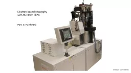
Electronbeam lithography with the Raith EBPG Part 1 Introduction M Rooks Yale University The EBPG has a long history stretching back to the 1960s This particular ebeam system was first built by Philips in the Netherlands then was bought out by Cambridge Instruments UK which morphed i ID: 773387
Download Presentation The PPT/PDF document "Electron-beam lithography" is the property of its rightful owner. Permission is granted to download and print the materials on this web site for personal, non-commercial use only, and to display it on your personal computer provided you do not modify the materials and that you retain all copyright notices contained in the materials. By downloading content from our website, you accept the terms of this agreement.

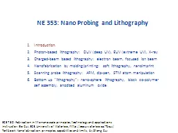


Electron-beam lithography with the Raith EBPGPart 1: Introduction M. Rooks, Yale University
The EBPG has a long history, stretching back to the 1960s. This particular e-beam system was first built by Philips (in the Netherlands), then was bought out by Cambridge Instruments (UK), which morphed into Leica Lithography, spun off as Vistec (and moved to the US), and now finally acquired by Raith (Germany). The EBPG is currently built in the Netherlands, where it began long ago. Throughout all this turmoil the EBPG has survived mostly due to customer loyalty and the commitment of a few key people in manufacturing and support.The Raith EBPG e-beam lithography system
This is a high-resolution Zeiss scanning electron microscope (SEM). It is the same one used in the low-end conversion kits sold by Raith, and it’s the same one that has generated linewidths less than 8 nm. The diagram shows a simplified view of the electron column. The scan coils are built for low noise, and so have very low bandwidth.
To convert a SEM into a writing instrument, one must insert a “beam blanker” in the column. The scan coils are controlled with a computer. Actually, the Zeiss SEM shown in the previous slide does not have two condenser lenses, and so the beam blanker has to go right inside the electron gun.
There are three big differences between a SEM and a big beam writer: speed, accuracy, and automation. The low bandwidth of SEM deflectors allows the instrument to write fine lines, but the catch is that those lines may not land where you want them. It’s like an uncertainty principle: low noise and low bandwidth lead to a larger uncertainty in placement, since the beam takes longer to settle after deflection. The SEM also has problems building large patterns out of small writing fields. If a pattern is built up from multiple exposure fields then the SEM will stitch those fields together poorly, compared to the dedicated system. Ease of use is a more subjective matter, but most people agree that the big systems are easier to use. They are certainly a lot faster, especially since they include automated calibration routines.
Because of the low bandwidth deflectors, converted SEMs often require patterns to include overlaps, so that patterns will not contain accidental gaps. Also, users often find it necessary to specify the order in which shapes are written, to minimize hysteresis effects. This is a serious disadvantage of using a converted SEM. (By the way, the e-beam system shown on the right is a JEOL 6300, which is a popular instrument in the US, but it’s not the one we have at Yale.) The table above states that the 100 kV system will require roughly 3 times the dose of electrons, but the high-voltage electron source is also three times brighter. In other words, lower resist sensitivity is offset by higher current. (“brightness” is the current in a given spot size)
Before we talk about our EBPG system, let’s go over the general strategy for e-beam lithography: Planning first, then design (CAD ). Complex devices, such as computer chips, are fabricated by printing patterns into a film called the “resist”, then transferring that pattern into the substrate (such as a silicon wafer). Hundreds of steps may be required to build commercial devices. Fortunately for research we usually build simple devices that require just a few printing steps.
As an example, let’s consider the design of a field-effect transistor (FET ), the fundamental building block of all computers. When the gate is charged positively, electrons are attracted toward it. These electrons change the region under the gate into a conductor, allowing current to pass from (let’s say) the left wire to the right. Or right to left - whatever. When the gate is not charged then the electrons under the gate dissipate and the transistor turns off. This is a typical device to build with electron-beam lithography, and it makes a nice example of how to organize your computer-aided design (CAD).
The various parts of a transistor are built up using a number of lithography steps, as shown here. Each step in the fabrication sequence is called a “layer” in the CAD program.
Here is the result of one layer of the design: the silicon has been patterned into an island (or “mesa”) to isolate it from other transistors.
Subsequent layers in the fabrication process follow, each including resist coating, exposure, development, and pattern transfer.
The pattern is exposed in resist (with electrons) then developed (e.g. with IPA/water). This pattern must then be transferred somehow to the substrate. You could etch the substrate in a plasma of reactive gas (e.g. chlorine) or you could evaporate metal and then strip the resist in a solvent. Other pattern transfer techniques include implantation and polishing.
Liftoff of metal wires requires soaking the wafer in solvents to “lift off” the unwanted metal. This is a common technique in research, usually employing PMMA resist. Liftoff is simple, but is not usually used in production, since there are more reliable and less messy ways of patterning wires. Acetone is a common solvent used for dissolving resist, and it becomes more effective if you heat it, b ut it also becomes explosive. Boiling acetone is foolish and unsafe. Instead use warm NMP, which works just as well, and can be heated up to 150C without becoming dangerously explosive.
E-beam resist choices Name Developer ~ Dose for 100 kV Positive* PMMA IPA:H 2 O 3:1, 7 °C 1000 m C /cm 2 ZEP xylenes, 10°C 600 CSAR Xylenes, 10°C 600 Negative* HSQ TMAH (MF312) 1000 ma-N TMAH (MF312)400 MultilayerPMMA on P(MMA-MAA)IPA:H2O 3:11000 HSQ on photoresistTMAH (MF319)1000PMMA/Ge/photoresistIPA:H2O 3:11000 * Positive The resist film will be removed where electrons hit Negative The resist film will remain only where electrons hit There are many other resists, but these are the most popular. The YINQE lab stocks PMMA, CSAR, and HSQ, in a variety of thicknesses.
E-beam resist developers PMMA and PMMA/copolymer IPA:water (3:1) at ~7°C is the best choice. (J. Vac. Sci. Techol. B 20(6) 2002). Older processes use MIBK:IPA mixtures, which are fine if you do not wish to re-engineer an established recipe. But IPA:water is better in every way, including being more environmentally friendly. We even recycle IPA/water for use in the cooling systems. HSQ This negative resist shrinks when exposed, and so develops considerable stress when exposed with a high dose. If you use a weak developer then the dose will be less and the stress will be less. But if you want the highest resolution then you need a strong developer. Our compromise is to use the TMAH solution “MF312” for most applications. For HSQ on polymer, there will be less stress and less delamination when developing in the weaker MF319 (or MF312 diluted 1:1 in water). For high resolution exposures or to reduce scum between lines, use the “MIT salty developer” (J. Vac. Sci. Technol. B 27(6), 2009). Alternatively, a strong 25% TMAH solution can be used, but this will readily etch silicon. On the other hand, 25% TMAH might attack your particular substrate slower than NaOH ; therefore you need to do some experimentation to determine which of these strong developers is best.
ZEP and CSAR These nearly identical resists are copolymers of methyl methacrylate and alpha methyl styrene. They can be developed in a wide assortment of chemicals, depending on your needs. There is a tradeoff between sensitivity (speed) and resolution. If you need to expose large features quickly, then you can use hexyl acetate as the developer. But most people use cold xylene to develop ZEP, when they need the best resolution. All of the developers cause swelling in the resist film, and so thick resist films will tend to form stress cracks. This limits resist thickness to about 1mm . ZEP and CSAR have better etch resistance than PMMA, but swelling during development limits the thickness and aspect-ratio of patterns. Beware: SEM images of this copolymer are always badly distorted due to resist flow. Most published images of ZEP and CSAR profiles are bogus. It’s still very good, high-resolution resist. Just don’t believe everything you read. (Except this page – you should believe this. ) E-beam resist developers, continued
Removing resist – what goes on must come off To remove… Use… But note that… PMMA Acetone or NMP You can heat NMP safely to 150 °C , but hot acetone is dangerously explosive. ZEP, CSAR NMP Liftoff is more difficult than with PMMA HSQ HF acid or CF 4 plasma HF is dangerous and etches most metals. Plasma etching can destroy the device. HSQ on polymer Acetone or NMP Use PMMA or photoresist baked at 180 °C as an underlayer – either for etch resistance, or just so you can strip off the HSQ without hurting the device.
E-beam on insulating substrates Au or Al PMMA or ZEP Quartz or sapphire Au or Al Water-soluble polymer HSQ Quartz or sapphire If your substrate is an insulator, such as quartz or sapphire, then you’ll need a conducting layer on top of the resist. For positive resists (PMMA) the conducting layer can simply be a 20 nm thick film of gold, deposited with a (slow) evaporator or with a (fast) table-top sputtering tool. You can expose the resist right through the metal film, then remove the film before development. Gold is easily removed in a solution of potassium iodide (“TFA gold etch”). When using HSQ resist you’ll need an extra layer of a water-soluble polymer, to keep the metal from mixing into the resist. One such polymer is PSSA , poly(4-styrenesulfonic acid ). Subtle point: The conducting layer will not keep the substrate from charging. A lot of charge will be deposited into the substrate, and it will not bleed away quickly. The conducting film is important because it acts as a shield to prevent the exposure beam from being deflected by the charged substrate. Therefore, it is not important that the metal film contact the substrate. Also note that there are conducting polymers that can be used instead of metal films, but these polymers are quite expensive and unstable. You can read more about this on nano.yale.edu/manuals-documentation. e-
Two common myths about e-beam resist PMMA cannot be used as an etch mask Not true. The only problem is the low glass transition temperature, 110°C. Simply keep the plasma etch power below 100W. ZEP and CSAR cannot be used for liftoff of metal Not true. The problem is that CSAR and ZEP do not dissolve well in acetone. Use warm NMP instead.
This is a classic picture showing how large features can be fully exposed while small features are underexposed. If this pattern were exposed at a higher dose, then the small features would develop properly while the large features bloom out and increase in size. This example is an exaggeration, since the pattern was exposed at 20kV. These days we are using 100kV electrons and the effects are much more subtle. For example, if you are writing a 300um wide grating, then the lines at the edges need about 10% higher dose than features in the middle. If you don’t care about the edges, then don’t worry about it! Are you worried?
Proximity effect Secondary electrons generated and scattered in the substrate contribute to the dose of other nearby features. How close is close? A 100 kV beam of electrons will scatter in silicon to a range around 26 m m (the 1/e range that is). This scattering can be simulated (as shown here) with a monte-carlo program such as “casino”. You might think that proximity effect would be less of a problem at low voltage, but that’s not the case. What matters is the ratio of primary electrons to secondary electrons. This ratio is higher at high voltage. Well, that’s not exactly true. When the voltage is below ~2 kV then the electrons will not even penetrate to the substrate, so at low voltage there is no proximity effect at all. Does this mean that low-voltage lithography is a good idea? No. You would be limited to a very thin resist layer, and alignment marks would be invisible.
Proximity effect What you have to worry about right away:Single-pixel features will need 5 to 10 times the dose of large features.Large pads will bleed over to small lines. You will have to set doses manually by assigning different doses to different datatypes or layers Automated proximity correction! You can use the pattern conversion program Beamer to calculate proximity exposure corrections, and to assign relative doses to shapes in your pattern. Sounds great! But it’s not as useful as you might think.
Proximity effect: bad news Dose correction with Beamer is simple enough, but it will help with only a very narrow range of problems. If the pattern is larger than ~ 50 um, contains a broad range of line widths, and is too complex for manual tweaking then it might help.If your resist is falling down, sticking together, or peeling off the substrate, then proximity effect correction will not help you.This presentation does not cover the use of Beamer for proximity correction. Just be aware that it exists, and ask about it later.
End of part I Now you should proceed to the quiz.