
University of Illinois UrbanaChampaign to Install First 150kV Electron Beam Lithography System in North America ID: 816854
Download Pdf The PPT/PDF document "University of Illinois Urbana-Champaign ..." is the property of its rightful owner. Permission is granted to download and print the materials on this web site for personal, non-commercial use only, and to display it on your personal computer provided you do not modify the materials and that you retain all copyright notices contained in the materials. By downloading content from our website, you accept the terms of this agreement.


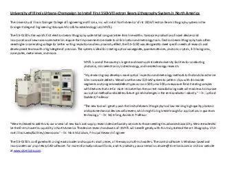
University of Illinois Urbana-Champaign to Install First 150kV Electron Beam Lithography System in North America The University of Illinois Grainger College of Engineering and Elionix, Inc. will install North Americaâs first 150kV Electron Beam Lithography system in the Grainger College of Engineering Holonyak Micro & Nanotechnology Lab (MNTL). The ELS-G150 is the worldâs first electron beam lithography system that can guarantee 4nm line widths. Nanoscale production of novel devices and incorporation of new nano-scale materials require that improvements be made to all fabrication and metrology tools. Electron beam lithography tools often need higher accelerating voltage for better writing resolution and less proximity effect; the ELS-G150 was designed to meet specific needs of research and development teams with a high degree of precision. The system is ideal for creating optical waveguides, quantum devices, photonic crystals, 3-D holograms, zone plates, meta-lenses, and more. MNTL is one of the countryâs largest and most sophisticated university facilities for conducting photonics, microelectronics, biotechnology, and nanotechnology research. âMy research group develops novel optical inspection and metrology methods to find and characterize killer nanoscale defects. We will use the new 150-keV system to pattern chips with 4-nm wide segments and programmed defect types across a 500 µm x 500 µm exposure field. Creating samples with features that are far more intricate than the current manufacturing node will enable us to improve our optical methods and address future grand challenges in the semiconductor industry.â â Dr. Lynford Goddard, Professor âThe new tool will greatly push the limit of ebeam lithography to allow realizing high-quality photonic and optomechanical devices unforeseen, which might bring breakthrough for applications in quantum technology.â â Dr. Kejie Fang, Assistant Professor âWe are pleased to add this to our arsenal of new tools and supply research device foundry services to those needing this advanced capability. We are excited to be the first to have this capability in North America. The device research and users of HMNTL will benefit greatly with this truly state-of-the-art lithography. Visit mntl.illinois.edu/facilities/cleanroomsâ â Dr. Mark McCollum, Principal Research Engineer The ELS-G150 is configured with a single auto loader and supports small pieces, all the way up to 8-inch wafers. The control software is Windows-based and incorporates our proprietary CAD software. For more information about Elionix, and its products, you can email us at sales@sts-elionix.com or visit our website at www.sts-elionix.com . View & Download Original Source @ https://www.sts-elionix.com/university-of-illinois-urbana-champaign-to-install-first-150kv-electron-beam-lithography-system-in-north-america/