
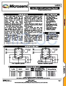
C VOUT1 VOUT2 Plastic MSOP 10PinRoHS Compliant Pbfree Transition DC 0432Package Marking 40 to 85 Adjustable AdjustableLX8221AIDU 8221 AIDU LX 40 to 85 25V AdjustableLX8221BIDU 8221 BIDU L ID: 837898
Download Pdf The PPT/PDF document "PACKAGE ORDER INFO" is the property of its rightful owner. Permission is granted to download and print the materials on this web site for personal, non-commercial use only, and to display it on your personal computer provided you do not modify the materials and that you retain all copyright notices contained in the materials. By downloading content from our website, you accept the terms of this agreement.


1 PACKAGE ORDER INFO C) VOUT1 VOUT2 Plast VOUT1 VOUT2
Plast")
PACKAGE ORDER INFO C) VOUT1 VOUT2 Plastic MSOP 10-PinRoHS Compliant / Pb-free Transition D/C: 0432Package Marking -40 to 85 Adjustable AdjustableLX8221AIDU 8221 AIDU LX -40 to 85 2.5V AdjustableLX8221BIDU 8221 BIDU LX -40 to 85 2.7V AdjustableLX8221DIDU 8221 DIDU LX -40 to 85 3.0V AdjustableLX8221GIDU8221 GIDU LX Note: Available in Tape & Reel. Append the letters TR to the part number. (i.e. LX8221AIDU-TR) 5.0V 3.3V To Control Logic Off EN1 APPLICATIONS Battery Operated Systems Laptop, Notebook and PDAs Cellular Telephones/Pagers Instrumentation Linear Post Regulators for PRODUCT HIGHLIGHT R1 To Control Logic Off EN1 EN2VOUT1VOUT2GNDADJCB1VIN1VIN2N/CAdjustable / Adjustable Application Microsemi Integrated Products Division 11861 Western Avenue, Garden Grove, CA. 92841, 714-898-8121, Fax: 714-893-2570 Copyright 2000 Rev. 1.1a, 2006-01-19 WWW.Microsemi COM Dual 150mA CMOS Low Dropout Re g ulator RODUCTION ATA TM The LX8221 family of dual output linear regulators provide for the selection of either fixed or adjustable output voltages, and combine low dropout operation, fast transient performance, tight output voltage accuracy, and ultra-low ground current IMPORTANT: For the most current data, consult Microsemis website: http://www.microsemi.com KEY FEATURES EN2VOUT1VOUT2ADJCB1VIN1VIN2Fixed / Adjustable Application R1 5.0V 3.3V Microsemi Integrated Products Division 11861 Western Avenue, Garden Grove, CA. 92841, 714-898-8121, Fax: 714-893-2570 Copyright 2000 Rev. 1.1a, 2006-01-19 WWW.Microsemi COM Dual 150mA CMOS Low Dropout Re g ulator RODUCTI
2 ON ATA TM ABSOLUTE MAXIMUM RATINGS Inp
ON ATA TM ABSOLUTE MAXIMUM RATINGS Input Voltage (VIN1, VIN2)..........................................................................-0.3V to +7V Output Current (I)................................................................................. 150mA Operating Temperature RangeMaximum Junction Temperature (T)......................................................................150 Storage Temperature (T).............................................................................-65 toPeak Package Solder Reflow Temp. (40 second max. exposure).................260°C (+Exceeding these ratings could cause damage to the device. All voltages are with respect to Ground. Currents are positive into, negative out of specified terminal. PACKAGE PIN OUT 24378 VIN1EN1ADJVOUT2VOUT1CB1EN2VIN2ACKAGE(Top View) NC = No Internal Connection RoHS / Pb-free 100% Matte Tin Lead Finish THERMAL DATA Plastic MSOP 8-Pin THERMAL RESISTANCEJUNCTION TO Junction Temperature Calculation: T = T + (P numbers are guidelines for the thermal performance of the device/pc-board system. All of the above assume no ambient airflow. FRONT MARKING 8221x = Voltage Combination FUNCTIONAL PIN DESCRIPTION IN ESCRIPTION VIN1/VIN2 Unregulated input supply voltage GND Ground Pin EN1/EN2 Enable control input: Logic high = Enable; logic low or open = Shutdown CB1 Reference bypass input. Adding an additional external capacitor reduces output noise. VOUT1/VOUT2 Regulated output voltage. Regulator stability is achieved with external capacitor of 1µF ADJ (1, 2) Adjust pin. Connect a resi
3 stor divider to this pin to establish pr
stor divider to this pin to establish preferred output voltage. BLOCK DIAGRAM VOUT1 - CONTROLLOGIC THERMALSENSOR LIMIT VREF VIN1 - CONTROLLOGIC THERMALSENSOR CURRENTLIMIT VIN2 VOUT2 PACCKKAAGGEE DATTAA Microsemi Integrated Products Division 11861 Western Avenue, Garden Grove, CA. 92841, 714-898-8121, Fax: 714-893-2570 Copyright 2000 Rev. 1.1a, 2006-01-19 WWW.Microsemi COM Dual 150mA CMOS Low Dropout Re g ulator RODUCTION ATA TM RECOMMENDED OPERATING CONDITIONS LX8221 Parameter Symbol Min Typ Max Input Operating Voltage Range (Note 1) VIN1, VIN2 2.5 6 V Enable Input Voltage Range EN1/2 V + 0.3VV Continuous Output Current Range I 150 mA Input Capacitor (V to GND) C 1.0* µF Output Capacitor (V to GND) C 1.0* 2.2 µF Note 1: The minimum V has to meet two conditions V 2.5V and V + VDROPOUT, at high line voltage conditions output current may be limited to less than 150mA due to the power dissipation. * Size your output capacitor to meet the transient loading requirement. If you have a very dynamic load, a lower ESR and larger value capacitor will improve the response to these load steps. ELECTRICAL CHARACTERISTICS Unless otherwise specified, the following specifications apply over the operating ambient temperature -40 85C except where otherwise noted. Test conditions: IN + 0.5VOUT =10mA = 1F; T = T using low duty cycle pulse testing methods. LX8221 Parameter Symbol Test Conditions Min Typ Max = 25°C -1 1 Output Voltage (2.5, 2.7, 3.0, ADJ) VOUT1/2 OUT1/2 OUT1/2 V -2.5 2.5 = 25°C 1.163 1.187 Adjust Reference Voltage V OUT1/2 100mA, 2.85V V
4 1.175 1.210 Line Regulation (VOUT1/2
1.175 1.210 Line Regulation (VOUT1/2 V OUT1/2 = 0.1mA 0.04 0.15 %/V = 25°C, 0.5mA OUT1/2 0.5 Load Regulation OOIV V OUT1/2 100mA 1.5 LOAD1/2 0.050 LOAD1/2 = -1% 0.175 LOAD1/2 = 100mA, 0.175 0.3 Dropout Voltage (Note 2)LOAD1/2 = 150mA, 0.25 0.4 EN1= High 280 440 Ground Pin Current STBY EN1= Low, EN2= Low 1 Adjust Input Bias Current I = 1.25V 100 nA Enable Pin Current IEN1/2 100 nA EN(IH) 2.0 Enable Threshold EN(IL) 0.4 Short Circuit Current Limit IOUT(SC) VOUT1 = 0V, VOUT2 = 0V 400 mA Power Supply Rejection Ratio T = 25°C, f = 120Hz 50 dB Output Noise e TBYPASS = 470pF 50 µV Thermal Shutdown Temperature T 170 °C Note 2: Dropout voltage is defined as the input to output differential at which the output voltage drops 1% below the nominal value. Dropout voltage specification applies only to output voltages greater than 2.8V. For output voltages below 2.8V, the dropout voltage is nothing but the input to output differential, since the minimum input voltage is 2.8V. ELEECCTTRRIICCAALLSS Microsemi Integrated Products Division 11861 Western Avenue, Garden Grove, CA. 92841, 714-898-8121, Fax: 714-893-2570 Copyright 2000 Rev. 1.1a, 2006-01-19 WWW.Microsemi COM Dual 150mA CMOS Low Dropout Re g ulator RODUCTION ATA TM Description The LX8221 family of LDO linear regulators is available in a 10-pin MSOP Package and provides a cost effective power management solution for battery driven applications. The regulator family includes both fixed/adjustable and adjustable/adjustable output voltage versions. The internal PMOS power device
5 provides low dropout regulation with a
provides low dropout regulation with a fast line and load transient response. It also includes internal current limiting and thermal shutdown circuitry. In this section you will find information about capacitor, thermal, and layout design considerations. Input Capacitor To improve load transient response and noise rejection a bypass capacitor is recommended (but it is not required for stability). There are no requirements for the ESR (Equivalent Series Resistor) on the input capacitor, but tolerance and temperature coefficient must be considered when selecting this capacitor to ensure that the capacitors value will be around 1F over the entire operating temperature range. For the LX8221, a 1F ceramic type capacitor may be connected between both VIN1/2 and ground. Output Capacitor The LX8221 uses an internal feedback loop to maintain a constant output voltage. This feedback loop induces a natural phase shift and the amount of phase shift determines the loops stability. Therefore, like any low-dropout regulator, an output capacitor with low ESR (Equivalent Series Resistance) is required between VOUT and GND to stabilize the internal control loop. A ceramic, tantalum or electrolytic capacitor with a minimum recommended capacitance value of 1.0F and ESR between and 1 will satisfy the stability for the entire operating range. Optional Bypass Capacitor The fixed/adjustable voltage version of the LX8221 includes a separate Bypass pin (CB1) for the fixed regulator that allows for further reduction of output noise. If the regulators output noise performance meets system design spec
6 ifications without the capacitor, omit i
ifications without the capacitor, omit it. The bypass capacitor impacts the start up time, which is inversely proportional to the size of bypass capacitor. Further, the bypass capacitor reduces the regulator phase margin. Hence, implementing the bypass capacitor will require the use of a larger output capacitor to maintain the LDOs stability. The LX8221-x adjustable regulators output voltage can be externally set by connecting the ADJ pin/s to an external resistor divider (See Figure 1 and 2). The output voltage can be calculated using the formula: EnableThe Enable pin allows the LX8221 to be independently turned on and off. The Enable pins are compatible with standard TTL-CMOS levels. A logic zero (0.4V) on the En pins shuts the LX8221 off and reduces the supply current to less than 1µA (typical). Pulling the Enable inputs high (2.0V) causes normal operation to resume. If the Enable feature is not used, this pin can be connected to VMinimum Load Requirement Although line regulation is improved with a minimum load of 100µA, the LX8221 does not have a minimum load current in order to maintain stability. This is an especially important feature in certain applications.Temperature Protection The thermal protection shuts the LX8221 down when the junction temperature exceeds approximately 150°C; there is no appreciable thermal hysteresis. Short Circuit Current Protection The LX8221 includes over-current protection, when the output load current exceeds about 400mA. When this occurs, the protection circuit forces the regulator to decrease its output current. Thermal Consideration
7 Thermal shutdown protects the integrate
Thermal shutdown protects the integrated circuit from thermal overload caused from a rise in junction temperature during power dissipation. This type of protection is intended for fault protection only and not as a means of current (or, power) limiting during normal application usage. Proper thermal evaluation should be done to ensure that the junction temperature dose not exceed its maximum rating. Operating at the maximum T of 150°C can impact reliability. Due to variation in individual device electrical characteristics and thermal resistance, the built in thermal overload protection may be activated at power levels slightly above or below the rated dissipation. Power dissipation for each regulator can APPPLLIICCAATTIIOONNSS Microsemi Integrated Products Division 11861 Western Avenue, Garden Grove, CA. 92841, 714-898-8121, Fax: 714-893-2570 Copyright 2000 Rev. 1.1a, 2006-01-19 WWW.Microsemi COM Dual 150mA CMOS Low Dropout Re g ulator RODUCTION ATA TM be calculated using the following equation: (Note: power dissipation resulting from quiescent current is negligible) For the MSOP package, thermal resistance, is 206°C/W when mounted on a FR4 copper clad PCB. Junction temperature of the integrated circuit can be calculated using: Where: Example: Given the following conditions: = 100mAcalculate the total power dissipation and junction temperature: Total Power Dissipation: Junction Temperature: Layout Consideration: The layout must be implemented with low impedance paths for V and Ground by creating sufficiently wide traces to avoid voltage drops and pick up noise. Add
8 ing an area of PCB copper to the GND pin
ing an area of PCB copper to the GND pin (pin 8) will reduce the overall since it is thermally connected to the device substrate. This will lower the device junction temperature improving overall output voltage accuracy. The input/output capacitors must be placed as close as possible to each voltage regulator output pin. APPPLLIICCAATTIIOONNSS Microsemi Integrated Products Division 11861 Western Avenue, Garden Grove, CA. 92841, 714-898-8121, Fax: 714-893-2570 Copyright 2000 Rev. 1.1a, 2006-01-19 WWW.Microsemi COM Dual 150mA CMOS Low Dropout Re g ulator RODUCTION ATA TM APPLICATION CIRCUITS R1 2.7V Resistor TableR1 = 13.0kR2 = 10.0k EN1 EN2VOUT1VOUT2VIN1VIN2N/C Figure 1 Fixed / Adjustable Output Application R1 2.7V2.5V Resistor TableVOUT1R1 = 13.0kR2 = 10.0kVOUT2R1 = 11.3kR2 = 10.0k EN1 EN2VOUT1VOUT2CB1VIN1VIN2N/C Figure 2 Adjustable / Adjustable Output Application APPPLLIICCAATTIIOONNSS Microsemi Integrated Products Division 11861 Western Avenue, Garden Grove, CA. 92841, 714-898-8121, Fax: 714-893-2570 Copyright 2000 Rev. 1.1a, 2006-01-19 WWW.Microsemi COM Dual 150mA CMOS Low Dropout Re g ulator RODUCTION ATA TM OUTPUT VOLTAGE VS TEMPERATURE DROPOUT VOLTAGE VS TEMPERATURE -50-250255075100125Temperature (°C)Output Voltage (V) 100125150175200225250275300325350-50-250255075100125TEMPERATURE (°C)=150mA=100mADropout (mV) OUTPUT CURRENT VS SUPPLY VOLTAGE SHORT CIRCUIT CURRENT VS TEMPERATURE -250-200-150-100-502.83.33.84.34.85.35.86.3Supply Voltage (V)-40°C25°C85°C115°CCurrent -430-420-400-390-380-370-360-350-340-40-2502585100115125Temperature (°C)Current (m
9 A) PSRR VS FREQUENCY PSRR VS FREQUENCY
PSRR VS FREQUENCY
PSRR VS FREQUENCY")
A) PSRR VS FREQUENCY PSRR VS FREQUENCY IN DROPOUT 1000.11Frequency(kHz) PSRR (dB)10100 0.1110100Frequency (kHz)PSRR (dB) Typical performance characteristics, unless otherwise specified are: C = C = 470pF, V = 2.5V, T = 25°C, ENABLE is tied to V Microsemi Integrated Products Division 11861 Western Avenue, Garden Grove, CA. 92841, 714-898-8121, Fax: 714-893-2570 Copyright 2000 Rev. 1.1a, 2006-01-19 WWW.Microsemi COM Dual 150mA CMOS Low Dropout Re g ulator RODUCTION ATA TM PACKAGE DIMENSIONS 10-Pin Plastic MSOP Lead Coplanarity ILLIMETERS MIN MAX MIN MAX A 2.85 3.05 0.112 0.120 B 2.90 3.10 0.114 0.122 C - 1.10 - 0.043 D 0.16 0.31 0.006 0.0124 F 0.40 0.60 0.015 0.023 G 0.50 BSC 0.019 BSC H 0.050 0.150 0.002 0.006 J 0.10 - 0.004 - P 4.75 5.05 0.187 0.198 *LC - 0.10 - 0.004 Note: protrusions; these shall not exceed 0.155mm(.006) on any side. Lead dimension shall MECCHHAANNIICCAALLSS Microsemi Integrated Products Division 11861 Western Avenue, Garden Grove, CA. 92841, 714-898-8121, Fax: 714-893-2570 Copyright 2000 Rev. 1.1a, 2006-01-19 WWW.Microsemi COM Dual 150mA CMOS Low Dropout Re g ulator RODUCTION ATA TM PRODUCTION DATA Information contained in this document is proprietary to Microsemi and is current as of publication date. This document may not be modified in any way without the express written consent of Microsemi. Product processing does not necessarily include testing of all parameters. Microsemi reserves the right to change the configuration and performance of the product and to discontinue product at any time. NOTTEESS