/
CSE 325 : Computer Peripherals and Interfacing CSE 325 : Computer Peripherals and Interfacing

CSE 325 : Computer Peripherals and Interfacing - PowerPoint Presentation

tabitha
tabitha . @tabitha
Follow
65 views
Uploaded On 2023-11-11

CSE 325 : Computer Peripherals and Interfacing - PPT Presentation

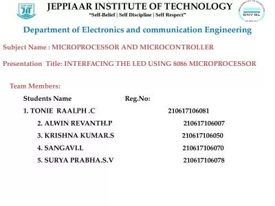
Sheikh Sujan Ali Associate Professor Dept of Computer Science and Engineering Jatiya Kabi Kazi Nazrul Islam University Mymensingh Bangladesh Introduction Computer Peripherals ID: 1031086

input port output data port input data output 82c55 bit mode figure device address microprocessor logic interface devices ports

Share:

Link:

Embed:

Download Presentation from below link

Download Presentation The PPT/PDF document "CSE 325 : Computer Peripherals and Inter..." is the property of its rightful owner. Permission is granted to download and print the materials on this web site for personal, non-commercial use only, and to display it on your personal computer provided you do not modify the materials and that you retain all copyright notices contained in the materials. By downloading content from our website, you accept the terms of this agreement.


Presentation Transcript

1. CSE 325:Computer Peripherals and InterfacingSheikh Sujan AliAssociate ProfessorDept. of Computer Science and EngineeringJatiya Kabi Kazi Nazrul Islam UniversityMymensingh, Bangladesh

2. IntroductionComputer PeripheralsA computer peripheral is any external device that provides input and output for the computer. For example, a keyboard and mouse are input peripherals, while a monitor and printer are output peripherals. Computer peripherals, or peripheral devices, are sometimes called I/O devices because they provide input and output for the computer. Some peripherals, such as external hard drives, USB flash drive and memory card provide both input and output for the computer.

3. Computer InterfacingIn computing, an interface is an art of connecting computers and peripherals by which two or more separate components of a computer system can exchange information. The exchange can be between software, computer hardware, peripheral devices, humans and combinations of these. The goal of this course is to introduce hardware and software design techniques and issues for interfacing computers and peripheral devicesIntroduction

4. Basic I/O InterfaceA microprocessor is great at solving problem, but can not communicate with the outside world.This chapter outlines some of the basic methods of communications, both serial and parallel, between humans or machines and the microprocessor.First introduces the basic I/O interface and discuss decoding for I/O devices. Then, provides detail on parallel and serial interfacing, both of which have a variety of applications.

5. Basic I/O Interfaces The basic input device is a set of three-state buffers. The basic output device is a set of data latches. The term IN refers to moving data from the I/O device into the microprocessor andThe term OUT refers to moving data out of the microprocessor to the I/O device.

6. Chapter Objectives Upon completion of this chapter, you will be able to: Explain the operation of the basic input and output interfaces.Decode an 8-, 16-, and 32-bit I/O device so that they can be used at any I/O port address.Define handshaking and explain how to use it with I/O devices.Interface and program the 82C55 programmable parallel interface.Interface LCD displays, LED displays, keyboards, ADC, DAC, and various other devices to the 82C55.Interface an analog-to-digital converter and a digital-to-analog converter to the microprocessor.Interface both DC and stepper motors to the microprocessor.

7. The I/O Instructions One type of instruction* transfers information to an I/O device (OUT). [*In computer science, an instruction is a single operation of a processor defined by the processor instruction set.]Another reads from an I/O device (IN).Instructions are also provided to transfer strings of data between memory and I/O.Instructions that transfer data between an I/O device and the microprocessor’s accumulator (AL, AX, or EAX) are called IN and OUT.

8. The I/O InstructionsThe I/O address is stored in register DX as a 16-bit address or as an 8-bit address. Intel calls the 8-bit form (p8) a fixed address The 16-bit address is called a variable address because it is stored in a DX, and then used to address the I/O device. Other instructions that use DX to address I/O are the INS and OUTS instructions.I/O ports are 8 bits in width.a 16-bit port is actually two consecutive 8-bitports being addressed a 32-bit I/O port is actually four 8-bit ports

9. The I/O InstructionsWhen data are transferred using IN or OUT, the I/O address, (port number or simply port), appears on the address bus. External I/O interface decodes the port number in the same manner as a memory address. the 8-bit fixed port number (p8) appears on address bus connections A7–A0 with bits A15–A8 equal to 000000002 The 16-bit variable port number (DX) appears on address connections A15–A0.

10. The I/O InstructionsINS and OUTS instructions address an I/O device using the DX register.but do not transfer data between accumulator and I/O device as do the IN/OUT instructionsInstead, they transfer data between memory and the I/O device

11. Isolated and Memory-Mapped I/O Two different methods of interfacing I/O: - isolated I/O and - memory-mapped I/O. In isolated I/O, the IN, INS, OUT, and OUTS transfer data between the microprocessor’s accumulator or memory and the I/O device. In memory-mapped I/O, any instruction that references memory can accomplish the transfer.

12. Isolated I/O The most common I/O transfer techniqueused in the Intel-based system is isolated I/O. isolated describes how I/O locations are isolated from memory in a separate I/O address space Addresses for isolated I/O devices, called ports, are separate from memory. Because the ports are separate, the user can expand the memory to its full size without using any of memory space for I/O devices.

13. Isolated I/O A disadvantage of isolated I/O is that data transferred between I/O and microprocessor must be accessed by the IN, INS, OUT, and OUTS instructions. Separate control signals for the I/O space are developed (using M/IO and W/R ), which indicate an I/O read (IORC) or an I/O write (RD) operation. These signals indicate an I/O port address, which appears on the address bus, is used to select the I/O device.

14. Memory and I/O Mapsin the PC, isolated I/Oports are used to control peripheral devices an 8-bit port address is used to access devices located on the system board, such as the timer and keyboard interfacea 16-bit port is used to access serial and parallel ports, video and disk drive systemsFigure:  The memory and I/O maps for the 8086/8088 microprocessors. (a) Isolated I/O. (b) Memory-mapped I/O.

15. Memory-Mapped I/O Memory-mapped I/O does not use the IN, INS, OUT, or OUTS instructions. It uses any instruction that transfers data between the microprocessor and memory. treated as a memory location in memory mapAdvantage is any memory transfer instruction can access the I/O device. Disadvantage is a portion of memory system is used as the I/O map.reduces memory available to applications

16. The Basic Input Interface Three-state buffers are used to construct the 8-bit input port depicted in Figure 2. External TTL data are connected to the inputs of the buffers. buffer outputs connect to the data bus The circuit of allows the processor to read the contents of the eight switches that connect to any 8-bit section of the data bus when the select signal becomes a logic 0.

17. Figure 2  The basic input interface illustrating the connection of eight switches. Note that the 74ALS244 is a three-state buffer that controls the application of the switch data to the data bus.

18. The Basic Input Interface When the IN instruction executes, contents of the switches copy to the AL register.To interface 16-bit of data, the circuit in Figure 2 is doubled to include to 74ALS244 buffers that connect 16 bits of input data to 16-bit data bus. To interface 32 bits of data, the circuit is expanded by a factor of 4.

19. The Basic Output InterfaceReceives data from the processor and usually must hold it for some external device. latches or flip-flops, like buffers in the inputdevice, are often built into the I/O deviceFig 3 shows how eight light-emitting diodes (LEDs) connect to the processor through a set of eight data latches. The latch stores the number output by the microprocessor from the data bus so that the LEDs can be lit with any 8-bit binary number.

20. Figure 3  The basic output interface connected to a set of LED displays.

21. The Basic Output InterfaceLatches hold the data because when the processor executes an OUT, data are only present on the data bus for less than 1.0 µs.the viewer would never see the LEDs illuminateWhen the OUT executes, data from AL, AX, or EAX transfer to the latch via the data bus. Each time the OUT executes, the SEL signal activates, capturing data to the latch.data are held until the next OUTWhen the output instruction is executed, data from the AL register appear on the LEDs.

22. Handshaking Many I/O devices accept or release information slower than the microprocessor. A method of I/O control called handshaking or polling, synchronizes the I/O device with the microprocessor. An example is a parallel printer that prints a few hundred characters per second (CPS). The processor can send data much faster.a way to slow the microprocessor down to match speeds with the printer must be developed

23. Handshaking Fig 4 illustrates typical input and output connections found on a printer. data transfers via data connections (D7–D0)ASCII data are placed on D7–D0, and a pulse is then applied to the STB connection.BUSY indicates the printer is busy STB is a clock pulse used to send data to printerThe strobe signal sends or clocks the data into the printer so that they can be printed.as the printer receives data, it places logic 1 on the BUSY pin, indicating it is printing data

24. Figure 4  The DB25 connector found on computers and the Centronics 36-pin connector found on printers for the Centronics parallel printer interface.

25. Handshaking The software polls or tests the BUSY pin to decide whether the printer is busy. If the printer is busy, the processor waitsif not, the next ASCII character goes to the printer This process of interrogating the printer, or any asynchronous device like a printer, is called handshaking or polling.

26. Input Devices Input devices are already TTL and compatible, and can be connected to the microprocessor and its interfacing components.or they are switch-basedSwitch-based devices are either open or connected; These are not TTL levels.TTL levels are a logic 0 (0.0 V–0.8 V)or a logic 1 (2.0 V–5.0 V)Using switch-based device as TTL-compatible input requires conditioning applied.

27. Input Devices Fig 5 shows a toggle switch properly connected to function as an input device.A pull-up resistor ensures when the switch is open, the output signal is a logic 1.when the switch is closed, it connects toground, producing a valid logic 0 levelA standard range of values for pull-up resistors is between 1K Ohm and 10K Ohm.

28. Input Devices Figure 5 A single-pole, single-throw switch interfaced as a TTL device.

29. Input Devices Mechanical switch contacts physically bounce when they are closed, which can create a problem if a switch is usedas a clocking signal for a digital circuitTo prevent problems with bounces, one of the circuits shown in Fig 7 can be used. the first is a classic textbook bounce eliminatorsecond is a more practical version of the same The first version costs more to constructthe second costs requires no pull-up resistorsand two inverters instead of two NAND gates

30. Bouncing ProblemSwitch Bouncing in Pull Down ConnectionSwitch Bouncing in Pull Up Connection

31. Figure 6  Debouncing switch contacts: (a) conventional debouncing and (b) practical debouncing.as the Q input from the switch becomes a logic 0, it changes the state of the flip-flopif the contact bounces away from the Q input, the flip-flop remembers, no change occurs, and thus no bounce

32. Output Devices Output devices are more diverse than input devices, but many are interfaced in a uniform manner. Before an output device can be interfaced, we must understand voltages and currents from the microprocessor or TTL interface.Voltages are TTL-compatible from the microprocessor of the interfacing element.logic 0 = 0.0 V to 0.4 Vlogic 1 = 2.4 V to 5.0 V

33. Output Devices Currents for a processor and many interfacing components are less than for standard TTL.Logic 0 = 0.0 to 2.0 mAlogic 1 = 0.0 to 400 µAFig 8 shows how to interface a simple LED to a microprocessor peripheral pin.a transistor driver is used in 8

34. Output Devices Figure 8  Interfacing an LED: using a transistor and.

35. Output Devices TTL input signal has minimum value of 2.4 V Drop across emitter-base junction is 0.7 V. The difference is 1.7 Vthe voltage drop across the resistor The value of the resistor is 1.7 V ÷ 0.1 mA or 17K W. as 17K W is not a standard value, an 18K W resistor is chosen

36. Output Devices In 8, we elected to use a switching transistor in place of the TTL buffer. 2N2222 is a good low-cost, general-purpose switching transistor with a minimum gain of 100 collector current is 10 mA; so base current willbe 1/100 of collector current of 0.1 mATo determine the value of the base current–limiting resistor, use the 0.1 mA base current and a voltage drop of 1.7 V across the base current–limiting resistor.

37. Output Devices Fig 9 illustrates a motor connected to the Darlington-pair with a minimum current gain of 7000 and a maximum current of 4A. Value of the bias resistor is calculated exactly the same as the one used in the LED driver. The current through the resistor is 1.0 A ÷ 7000, or about 0.143 mA.Voltage drop is 0.9 V because of the two diode drops (base/emitter junctions). The value of the bias resistor is 0.9 V ÷ 0.143 mA or 6.29K W.

38. Figure 9  A DC motor interfaced to a system by using a Darlington-pair.The Darlington-pair must usea heat sink because of theamount of currentthe diode must be present toprevent the Darlington-pairfrom being destroyed by inductive kickback

39. Darlington pairDarlington pair/transistor is a compound structure of a particular design made by two bipolar transistors connected in such a way that the current amplified by the first transistor is amplified further by the second one.Darlington transistors can be used in high-current circuits, such as those involving computer control of motors or relays.

40. DecoderIn digital electronics, a binary decoder is a combinational logic circuit that converts binary information from the n coded inputs to a maximum of 2n unique outputs.

41. Decoding 8-Bit I/O Port Addresses Fixed I/O instruction uses an 8-bit I/O port address that on A15–A0 as 0000H–00FFH.we often decode only address connectionsA7–A0 for an 8-bit I/O port addressThe DX register can also address I/O ports 00H–FFH. If the address is decoded as an 8-bit address, we can never include I/O devices using a 16-bit address. the PC never uses or decodes an 8-bit address

42. Decoding 8-Bit I/O Port Addresses Figure 10 shows a 74ALS138 decoder that decodes 8-bit I/O ports F0H - F7H. identical to a memory address decoder exceptwe only connect address bits A7–A0 to theinputs of the decoderFigure 11 shows the PLD version, using a GAL22V10 (a low-cost device) for this decoder. The PLD is a better decoder circuit because the number of integrated circuits has been reduced to one device.

43. Figure 10  A port decoder that decodes 8-bit I/O ports. This decoder generates active low outputs for ports F0H–F7H.

44. Figure 11  A PLD that generates port selection signals

45. Figure 12  A PLD that decodes 16-bit I/O ports EFF8H through EFFFH.

46. Figure 13  A 32-bit-wide port decoded at 70H through 73H for the 80486DX microprocessor.I/O ports decoded by this interface are the 8-bit ports 70H–73HWhen writing to access this port, it is crucial to use the address 70H for 32-bit inputas instruction IN EAX, 70H

47. THE PROGRAMMABLE PERIPHERAL82C55 programmable peripheral interface (PPI) is a popular, low-cost interface component found in many applications. The PPI has 24 pins for I/O, programmable in groups of 12 pins and groups that operate in three distinct modes of operation. 82C55 can interface any TTL-compatibleI/O device to the microprocessor.

48. THE PROGRAMMABLE PERIPHERALThe 82C55 (CMOS version) requires wait states if operated with a processor using higher than an 8 MHz clock. also provides at least 2.5 mA of sink (logic 0) current at each output, a maximum of 4.0 mA Because I/O devices are inherently slow, wait states used during I/O transfers do not impact significantly upon the speed of the system.The 82C55 still finds application even in the latest Core2-based computer system.

49. THE PROGRAMMABLE PERIPHERAL82C55 is used for interface to the keyboard and parallel printer port in many PCs.found as a function within an interfacing chip setalso controls the timer and reads data from the keyboard interfaceAn experimentation board is available that plugs into the parallel port of a PC, to allow access to an 8255 located on the board. The 8255 is programmed in either assembly language or Visual C++ through drivers available with the board.

50. Basic Description of the 82C55 Fig 14 shows pin-outs of the 82C55 in DIP and surface mount (flat pack) format.The three I/O ports (labeled A, B, and C) are programmed as groups. group A connections consist of port A (PA7–PA0) and the upper half of port C (PC7–PC4)group B consists of port B (PB7–PB0) and the lower half of port C (PC3–PC0) 82C55 is selected by its CS pin for programming and reading/writing to a port.

51. Figure 14  The pin-out of the 82C55 peripheral interface adapter (PPI).

52. Basic Description of the 82C55 Table 1 shows I/O port assignments used for programming and access to the I/O ports. In the PC, a pair of 82C55s, or equivalents, are decoded at I/O ports 60H–63H and alsoat ports 378H–37BH.The 82C55 is a fairly simple device to interface to the microprocessor and program. For 82C55 to be read or written, the CS input must be logic 0 and the correct I/O address must be applied to the A1 and A0 pins. Remaining port address pins are don’t cares

53. Basic Description of the 82C55 Fig 15 shows an 82C55 connected to the 80386SX so it functions at 8-bit addresses C0H (port A), C2H (port B), C4H (port C),and C6H (command register). this interface uses the low bank of the I/O map All 82C55 pins are direct connections to the 80386SX, except the CS pin. The pin is decoded/selected by a 74ALS138 decoder.A RESET to 82C55 sets up all ports assimple input ports using mode 0 operation. initializes the device when the processor is reset

54. Figure 15  The 82C55 interfaced to the 80386SX microprocessor.

55. Basic Description of the 82C55 After a RESET, no other commands are needed, as long as it is used as an input device for all three ports. 82C55 is interfaced to the PC at port addresses 60H–63H for keyboard control.also for controlling the speaker, timer, and other internal devices such as memory expansion It is also used for the parallel printer port at I/O ports 378H–37BH.

56. Programming the 82C55 82C55 is programmed through two internal command registers shown in Figure 16.Bit position 7 selects either command byte A or command byte B. command byte A programs functions of group A and Bbyte B sets (1) or resets (0) bits of port C only if the 82C55 is programmed in mode 1 or 2Group B (port B and the lower part of port C) are programmed as input or output pins.

57. Figure 16 The command byte of the command register in the 82C55.

58. Programming the 82C55 Mode 0 : Simple Input or OutputIn this mode, Port A and Port B are used as two simple 8-bit I/O ports and Port C as two 4-bit I/O ports. Each port (or half-port, in case of Port C) can be programmed to function as simply an input port or an output port. The input/output features in mode 0 are :Outputs are latched, Inputs are not latched (?). Ports do not have handshake or interrupt capability.

59. Programming the 82C55 Mode 1 : Input or Output with handshakeIn mode 1, handshake signals are exchanged between the microprocessor and peripherals prior to data transfer. The ports (A and B) function as 8-bit I/O ports. They can be configured either as input or output ports. Each port (Port A and Port B) uses 3 lines from port C as handshake signals. The remaining two lines of port C can be used for simple I/O functions. Input and output data are latched and Interrupt logic is supported.

60. Programming the 82C55 Mode 2 : Bidirectional Data TransferThis mode is used primarily in applications such as data transfer between the two computers or floppy disk controller interface. Port A can be configured as the bidirectional port and Port B either in mode 0 or mode 1. Port A uses five signals from Port C as handshake signals for data transfer. The remaining three lines from Port C can be used either as simple I/O or as handshake signals for Port B.

61. Programming the 82C55 Group A (port A and the upper part of port C) are programmed as input or output pins. Group A can operate in modes 0, 1, and 2. mode 2 operation is a bidirectional mode of operation for port AIf a 0 is placed in bit position 7 of the command byte, command byte B is selectedThis allows any bit of port C to be set (1) or reset (0), if the 82C55 is operated in either mode 1 or 2. otherwise, this byte is not used for programming

62. Mode 0 Operation Mode 0 operation causes 82C55 to function:as a buffered input device as a latched output device Fig 17 shows 82C55 connected to a set of eight seven-segment LED displays. These are standard LEDs.the interface can be modified with a changein resistor values for an organic LED (OLED) display or high-brightness LEDs

63. Figure 17  An 8-digit LED display interfaced to the 8088 microprocessor through an 82C55 PIA

64. An 8-digit LED displayports A & B are programmed as (mode 0) simple latched output ports port A provides segment data inputs port B provides a means of selecting one display position at a time for multiplexing the displays the 82C55 is interfaced to an 8088 through a PLD so it functions at I/O port numbers 0700H–0703HPLD decodes the I/O address and develops the write strobe for the WR pin of the 82C55

65. A Stepper Motor Interfaced to the 82C55.Another device often interfaced to a computer system is the stepper motor. a digital motor because it is moved in discrete steps as it traverses through 360° An inexpensive stepper motor is geared to move perhaps 15° per stepA more costly, high-precision stepper motor can be geared to 1° per step.

66. A Stepper Motor Interfaced to the 82C55.In all cases, these steps are gained through many magnetic poles and/or gearing. Figure 18 shows a four-coil stepper motor that uses an armature with a single pole. two coils are energizedIf less power is required, one coil may be energized at a time, causing the motor tostep at 45°, 135°, 225°, and 315°.The motor is shown with the armature rotated to four discrete places, called full stepping. accomplished by energizing the coils, as shown

67. Figure 18 The stepper motor showing full-step operation: (a) 45° (b) 135° (c) 225° (d) 315°.

68. A Stepper Motor Interfaced to the 82C55.The motor is driven by NPN Darlington amp pairs to provide a large current to each coil.A circuit that can drive this stepper motor is illustrated in Fig 19.with the four coils shown in place This circuit uses the 82C55 to provide drive signals used to rotate the motor armature in either the right- or left-hand direction.

69. Figure 19  A stepper motor interfaced to the 82C55. This illustration does not show the decoder.

70. Key Matrix Interface Keyboards come in a variety of sizes, from standard 101-key QWERTY keyboards to special keyboards that contain 4 to 16 keys. Fig 20 is a key matrix with 16 switches interfaced to ports A and B of an 82C55. the switches are formed into a 4  4 matrix,but any matrix could be used, such as a 2  8The keys are organized into four rows and columns: (ROW0–ROW3) (COL0–COL3)

71. Figure 20 A 4  4 keyboard matrix connected to an 8088 microprocessor through the 82C55 PIA.

72. Mode 1 Strobed Input In computer or memory technology, a strobe is a signal that is sent that validates data or other signals on adjacent parallel lines.Causes port A and/or port B to function as latching input devices. allows external data to be stored to the portuntil the microprocessor is ready to retrieve it Port C is used in mode 1 operation—not for data, but for control or handshaking signals.to help operate either or both port A and B as strobed input ports Fig 21 shows how both ports are structured for mode 1 strobed input operation.

73. Signal Definitions for Mode 1 Strobed InputSTB - The strobe input loads data to the port latch, which holds the information until it is input to the microprocessor via the IN instruction. IBF - Input buffer full is an output indicating that the input latch contains information.INTR - Interrupt request is an output that requests an interrupt. The INTR pin becomes a logic 1 when STB returns to a logic 1. Cleared when data are input from the port by the processor.INTE - Interrupt enable signal is neither input nor output; it is an internal bit programmed via port PC4 (port A) or PC2 (port B) bit position.

74. Figure 21  Strobed input operation (mode 1) of the 82C55. (a) Internal structure and (b) timing diagram.

75. Strobed Input Example An example of a strobed input device is a keyboard. The keyboard encoder debounces the key switches and provides a strobe signal whenever a key is depressed.the data output contains ASCII-coded key codeFigure 22 illustrates a keyboard connected to strobed input port A.

76. Figure 22  Using the 82C55 for strobed input operation of a keyboard.

77. Mode 1 Strobed Output Fig 23 shows the internal configuration and timing diagram of 82C55 when operated as a strobed output device under mode 1. Strobed output operation is similar to mode 0 output operation.except control signals are included to provide handshakingWhen data are written to a strobed output port, the output buffer full signal becomes logic 0 to indicate data are present in the port latch.

78. Signal Definitions for Mode 1 Strobed OutputOBF - Output buffer full goes low whenever data are output (OUT) to the port A or B latch. The signal is set to logic 1 when the ACK pulse returns from the external device. ACK - The acknowledge signal causes the OBF pin to return to logic 1. The ACK signal is a response from an external device, indicating that it has received data from the 82C55 port. INTR - Interrupt request often interrupts the processor when the external device receives the data via the ACK signal. Qualified by the internal INTE (interrupt enable) bit. INTE - Interrupt enable is neither input nor output; it is an internal bit programmed to enable or disable the INTR pin. INTE A is programmed using PC6 bit. INTE B is programmed using the PC2 bit.

79. Figure 23  Strobed output operation (mode 1) of the 82C55. (a) Internal structure and (b) timing diagram

80. Strobed Output Example The printer interface demonstrates how to achieve strobed output synchronization between the printer and the 82C55. Figure 24 illustrates port B connected to a parallel printer, with eight data inputs for receiving ASCII-coded data, a DS (data strobe) input to strobe data into the printer, and an ACK output to acknowledge the receipt of the ASCII character.

81. Figure 24  The 82C55 connected to a parallel printer interface that illustrates the strobed output mode of operation for the 82C55.

82. Mode 2 Bidirectional Operation Mode 2 is allowed with group A only.Port A becomes bidirectional, allowing data transmit/receive over the same eight wires. useful when interfacing two computers Also used for IEEE-488 parallel high-speed GPIB (general- purpose instrumentation bus) interface standard.Figure 11-30 shows internal structure and timing for mode 2 bidirectional operation.

83. Figure 11-30  Mode 2 operation of the 82C55. (a) Internal structure and (b) timing diagram.

84. 82C55 Mode Summary Figure 26 shows a graphical summary of the three modes of operation for the 82C55.Mode 0 provides simple I/O.Mode 1 provides strobed I/O.Mode 2 provides bidirectional I/O.These modes are selected through the command register of the 82C55.

85. Figure 26  A summary of the port connections for the 82C55 PIA.

86. 8254 PROGRAMMABLE INTERVAL TIMER The 8254 consists of three independent 16-bit programmable counters (timers). Each counter is capable of counting in binary or binary-coded decimal (BCD). maximum allowable input frequency to any counter is 10 MHzUseful where the microprocessor must control real-time events.Usage includes real-time clocks, event counters, and motor speed/direction control.

87. 8254 Functional Description Figure 27 shows the pin-out of the 8254, a higher-speed version of the 8253, and a diagram of one of the three counters. Each timer contains:a CLK input which provides the basic operating frequency to the timer a gate input pin which controls the timer in some modesan output (OUT) connection to obtain the output of the timer

88. Figure 27  The 8254 programmable interval timer. (a) Internal structure and (b) pin-out. (Courtesy of Intel Corporation.)

89. 8254 Functional Description The signals that connect to the processor are the data bus pins (D7–D0), RD, WR, CS, and address inputs A1 and A0. Address inputs are present to select any of the four internal registers.used for programming, reading, or writing to a counterTimer zero generates an 18.2 Hz signal that interrupts the microprocessor at interrupt vector 8 for a clock tick. often used to time programs and events in DOS Timer 1 is programmed for 15 µs, used on the PC to request a DMA action used to refresh the dynamic RAM. Timer 2 is programmed to generate a tone on the PC speaker.

90. Pin Definitions for 8254-The address inputs select one of four internal registers within the 8254. See Table 11–4 for the function of the A1 and A0 address bits. CLK-The clock input is the timing source for each of the internal counters. This input is often connected to the PCLK signal from the microprocessor system bus controller. CS - Chip select enables 8254 for programming and reading or writing a counter. G - The gate input controls the operation of the counter in some modes of operation GND - Ground connects to the system ground bus.

91. Pin Definitions for 8254OUT - A counter output is where the waveform generated by the timer is available. RD - Read causes data to be read from the 8254 and often connects to the IORC signal.VCC - Power connects to the +5.0 V power supply. WR - Write causes data to be written to the 8254 and often connects to write strobe IOWC.

92. Programming the 8254 Each counter is programmed by writing a control word, followed by the initial count. fig 28 lists the program control word structure The control word allows the programmer to select the counter, mode of operation, and type of operation (read/write). also selects either a binary or BCD count

93. Figure 28  The control word for the 8254-2 timer.

94. Modes of Operation six modes (0–5) of available to each of the 8254 counters each mode functions with the CLK input, the gate (G) controlsignal, and OUT signalFigure 29  The six modes of operation for the 8254-2 programmable interval timer. The G input stops the count when 0 in modes 2, 3, and 4.

95. Mode 0 Allows 8254 to be used as an events counter. Output becomes logic 0 when the control word is written and remains until N plus the number of programmed counts. For example, if a count of 5 is programmed, the output will remain a logic 0 for 6 count beginning with N.Note that gate (G) input must be logic 1 to allow the counter to count. If G becomes logic 0 in the middle of the count, the counter will stop until G again becomes logic 1.

96. Mode 1 Causes function as a retriggerable, monostable multivibrator (one-shot). G input triggers the counter so it develops a pulse at the OUT connection that becomes logic 0 for the duration of the count. if the count is 10, the OUT connection goeslow for 10 clocking periods when triggered If G input occurs within the output pulse, the counter is reloaded and the OUT connection continues for the total length of the count.

97. Mode 2Allows the counter to generate a series of continuous pulses one clock pulse wide. pulse separation is determined by the count For a count of 10, output is logic 1 for nine clock periods and low for one clock period. The cycle is repeated until the counter is programmed with a new count or until the G pin is placed at logic 0. G input must be logic 1 for this mode togenerate a continuous series of pulses

98. Mode 3Generates a continuous square wave at the OUT connection, provided the G pin is logic 1.If the count is even, output is high for one half of the count and low for one half of the count. If the count is odd, output is high for one clocking period longer than it is low. if the counter is programmed for a count of 5, the output is high for three clocks and low for two clocks

99. Mode 4Allows a single pulse at the output. If count is programmed as 10, output is high for 10 clocking periods and low for one period. the cycle does not begin until the counteris loaded with its complete countOperates as a software triggered one-shot. As with modes 2 and 3, this mode also uses the G input to enable the counter. G input must be logic 1 for the counter tooperate for these three modes

100. Mode 5A hardware triggered one-shot that functions as mode 4.except it is started by a trigger pulse on theG pin instead of by softwareThis mode is also similar to mode 1 becauseit is retriggerable.

101. DC Motor Speed and Direction Control An application of 8254 is as a motor speed controller for a DC motor. Fig 11-45 shows the schematic diagram of the motor and associated driver circuitry. It also illustrates the interconnection of the 8254, a flip-flop, and the motor and its driver.Fig 11–46 shows some timing diagrams and effects on the speed/direction of the motor. Each counter generates pulses at different positions to vary the duty cycle at the Q output of the flip-flop.

102. DC Motor Speed and Direction Control

103. DC Motor Speed and Direction Control if Q output of the 74ALS112 is logic 1, the motor spins in its forward direction if logic 0, the motor spins in reverseif flip-flop output alternates betweenlogic 1 and 0, the motor spins in either direction at various speedsif the duty cycle of the Q output is 50%, the motor will not spin at all and exhibits some holding torque

104.

105. ANALOG-TO-DIGITAL (ADC) & DIGITAL-TO-ANALOG (DAC) CONVERTERSThese devices are used to interface the microprocessor to the analog world. Many events monitored and controlled by the microprocessor are analog events. These range from monitoring all forms of events, even speech, to controlling motors and like devices.

106. The DAC0830 Digital-to-Analog Converter A fairly common and low-cost digital-to-analog converter is the DAC0830.a product of National Semiconductor Corp An 8-bit converter that transforms an 8-bit binary number into an analog voltage. Other converters are available that convert from 10-, 12-, or 16-bit binary numbers into analog voltages.

107. The DAC0830 Digital-to-Analog Converter The number of voltage steps generated by the converter is equal to the number of binary input combinations. an 8-bit converter generates 256 voltage levelsa 10-bit converter generates 1024 levels The DAC0830 is a medium-speed converter that transforms a digital input to an analog output in approximately 1.0 µs.

108. The DAC0830 Digital-to-Analog Converter Figure 11–48 shows pin-outs of a DAC0830.The device has eight data bus connections for the application of the digital input code.Analog outputs labeled IOUT1 & IOUT2 are inputs to an external operational amplifier. Because this is an 8-bit converter, its output step voltage is defined as –VREF (reference voltage), divided by 255. the step voltage is often called the resolutionof the converter

109. Figure 11–48  The pin-out of the DAC0830 digital-to-analog converter.

110. Internal Structure of the DAC0830 Fig 11–49 shows the internal structure. This device contains two internal registers.the first is a holding registerthe second connects to the R–2R internal ladder converterThe two latches allow one byte to be held while another is converted. The first latch is often disabled and the second for entering data into the converter.

111. Figure 11–49  The internal structure of the DAC0830.

112. Both latches within the DAC0830 are transparent latches. when G input is logic 1, data pass throughwhen G input becomes logic 0, data are latched The output of the R–2R ladder within the converter appears at IOUT1 and IOUT2.These outputs are designed to be applied to an operational amplifier such as a 741 or similar device.

113. Connecting the DAC0830 to the Microprocessor. A PLD is used to decode the DAC0830 at I/O port address 20H. when an OUT 20H,AL instruction is executed, contents of data bus connections AD0–AD7 are passed to the converter in the DAC0830The 741 operational amplifier, along with the –12 V zener reference voltage, causes the full-scale output voltage to equal +12 V. See Fig 11–50.

114. Figure 11–50  A DAC0830 interfaced to the 8086 microprocessor at 8-bit I/O location 20H.

115. The ADC080X Analog-to-Digital ConverterA common, low-cost ADC, compatible with a wide range of microprocessors.while there are faster ADCs available with more resolution, this device is ideal for applicationsthat do not require a high degree of accuracy ADC080X requires up to 100 µs to convert an analog input voltage into a digital output code.Figure 11–51 shows the pin-out of the ADC0804 converter.

116. Figure 11–51  The pin-out of the ADC0804 analog-to-digital converter.

117. To operate the converter, the WR pin is pulsed with CS grounded to start the conversion process. See Fig 11–52 for a timing diagram that shows the interaction of the control signals.If a time delay is used that allows at least 100 µs of time, there is no need to test INTR pin.Another option is to connect the INTR pin to an interrupt input, so when the conversion is complete, an interrupt occurs.

118. Connecting the ADC0804 to the Microprocessor ADC0804 interfaced to an 8086 is illustratedin Figure 11–55. VREF is not attached to anything, which is normal Suppose ADC0804 is decoded at I/O port address 40H for the data and address 42Hfor INTR.The procedure to read data is listed in Example 11–29.

119. Figure 11–55  The ADC0804 interfaced to the 8086 microprocessor.

120. Using the ADC0804 and the DAC0830 This illustrates an example using an ADC0804 and a DAC0830 to capture and replay audio signals or speech. a speech synthesizer has been used in the pastto generate speech, but quality was poor For human quality speech, we can use an ADC0804 to capture an audio signal and store it for later playback through a DAC0830.

121. Figure 11–61  A circuit that stores speech and plays it back through the speaker.

122. A procedure called READS reads the speech.A second, PLAYS, plays it back.The speech is sampled and stored in a section of memory called WORDS. The sample rate is chosen at 2048 samples per second, which renders acceptable-sounding speech.