
From IBIS 60 The Pin Mapping keyword names the connections between POWER andor GND pins and buffer andor terminator voltage supply references using unique bus labels All buses with identical labels are assumed to be connected with an ideal short ID: 1003522
Download Presentation The PPT/PDF document "Pin Mapping Key Concepts" is the property of its rightful owner. Permission is granted to download and print the materials on this web site for personal, non-commercial use only, and to display it on your personal computer provided you do not modify the materials and that you retain all copyright notices contained in the materials. By downloading content from our website, you accept the terms of this agreement.


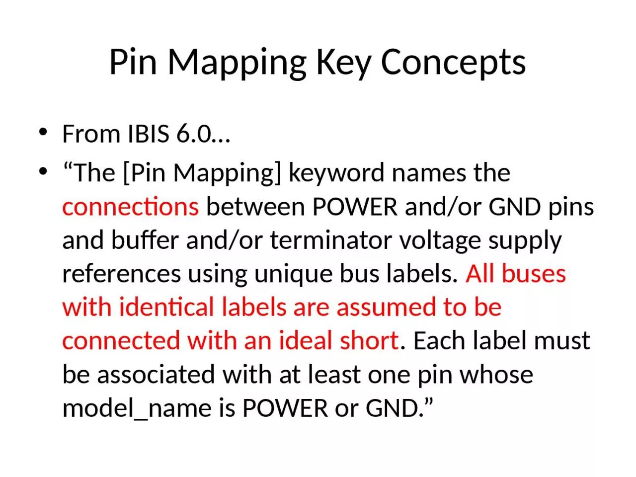
1. Pin Mapping Key ConceptsFrom IBIS 6.0…“The [Pin Mapping] keyword names the connections between POWER and/or GND pins and buffer and/or terminator voltage supply references using unique bus labels. All buses with identical labels are assumed to be connected with an ideal short. Each label must be associated with at least one pin whose model_name is POWER or GND.”
2. Key Concepts (cont’d)“The second column, pulldown_ref, designates the ground bus connections for the buffer or termination associated with that pin. The bus named under pulldown_ref is associated with the [Pulldown] I-V table for non-ECL [Model]s.”“The third column, pullup_ref, designates the power bus connection for the buffer or termination. The bus named under pullup_ref is associated with the [Pullup] table for non-ECL [Model]s…”
3. Pin Mapping in Interconnect BIRDIn Draft 9... “… all pins with Signal_name VDD [connect to] to all Buffer supply terminals that are connected to Signal_name VDD as described in Pin_mapping.”“All Pins with Signal_name VDD are shorted together. ““All Buffer supply terminals that are connected to Signal_name VDD are shorted together”
4. Example from Draft 9, P. 13 VDD: Interconnect between VDD Pins and individual buffer Pullup Reference.Terminal 1 Pin P1Terminal 2 Pin P2Terminal 3 Pin P3Terminal 4 Pin P4Terminal 5 Pin P5Terminal 6 Buf_PURef A1Terminal 7 Buf_PURef A2Terminal 8 Buf_PURef A3Terminal 9 Buf_PURef D1
5. ProposalDraft 9 and IBIS [Pin Mapping] agree on shorting of pins associated with a named supply[Pin] model_name must be POWER or GND[Pin Mapping] implies but does not state a direct connection (short) between the buffer supply rail and the pinSuggestion: For traditional interconnects, assume buffer rail/pin shortFor Draft 9 Interconnects([Interconnect Model] present), state that interconnect “sits between” buffer rail and pinPin Mapping rails still shorted to each otherPin Mapping pins on named supplies still shorted together
6. Additional IssueFrom IBIS 6.0…“If the [Pin Mapping] keyword is present, then the bus connections for EVERY pin listed under the [Pin] keyword must be given.” Does this prevent effective use of Draft 9 Interconnects?Partial interconnect descriptions become impossible