
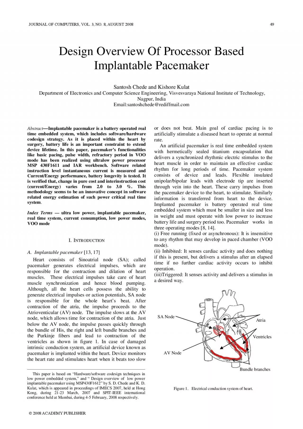
Ventricle s Atria AV Node SA Node Bundle branches This paper is based on 141Hardwaresoftware codesign techniques in low power embedded system142 and 141 Design overview of low powe r impla ID: 936588
Download Pdf The PPT/PDF document "Design Overview Of Processor Based Impla..." is the property of its rightful owner. Permission is granted to download and print the materials on this web site for personal, non-commercial use only, and to display it on your personal computer provided you do not modify the materials and that you retain all copyright notices contained in the materials. By downloading content from our website, you accept the terms of this agreement.


Design Overview Of Processor Based Implantable Pacemaker Santosh Chede and Kishore Kulat Department of Electronics and Computer Science Engineering, Visvesvaraya National Institute of Technology, Nagpur, India Email:santoshchede@rediffmail.com AbstractImplantable pacemaker is a battery operated real time embedded system, which includes software/hardware codesign strategy. As it is placed within the heart by surgery, battery life is an important constraint to extend device lifetime. In this paper, pacemakers functionalities like basic pacing, pulse width, refractory period in VOO Ventricle s Atria AV Node SA Node Bundle branches This paper is based on Hardware/software codesign techniques in low power embedded system,Ž and Design overview of low powe r implantable pacemaker using MSP430F1612Ž by S. D. Chede and K. D. Kulat, which is appeared in proceedings ofIMECS 2007, held at HongKong, during 21-23 March, 2007 and SPIT-IEEE internationa l conference held at Mumbai,durin g 4-5 Februar y ,2008 res p ectivel y . B. Pacemaker timing parameters Basic pace interval: The basic pace interval is the period of time that pacemaker awaits to apply stimulus to the heart. It is measured in beats/min. Escape interval: The escape interval is the period of time that the pacemaker awaits after a spontaneous QRS has been generated. It is measured in ms. Ventricular Refractory period (VRP): The VRP is the amount of time that the sense circuit is turned off. This is done to avoid sensing the pacemaker own stimulus, the paced
QRS complex, T wave and after potentials. If the sensing circuit is turned on, then it will generate stimuli to all these events, causing ventricular fibrillation. It is measured in msec. Pulse width: It is the amount of time the pulse generator will supply the stimulus to the heart. This parameter is important to capture heart. Capture is the action of generating a potential that develop chain reaction through out the ventricle. The pulse width is measured in msec. C. Modes of operation North American Society of Pacing and electrophysiology (NASPE) and British pacing and Electrophysiology (BPEG) used nomenclatures to classify pacemakers like VVI, VVT, VOO, AAI, AAT and AOO is given in table I [6]. VVI means pacemaker sense the ventricle and pace the ventricles in inhibited mode. VOO means an asynchronous mode in which ventricle is paced with no chamber sensed and no response to sensing i.e. irrespective of the heart signal, pacemaker generates pacing pulses. II.ACEMAKER ESIGN OALS ENCHMARKS EROS ODEL SSIR603[15] Pacing Modes: VVI, VVT, VOO, OVO, AAI, AAT, AOO, OAO, VVIR, VVTR, VOOR, AATR, AOOR, AAIR Basic Pacing Rates: From 32 to 120 bpm in steps of 2 bpm. Pulse Widths: 20 values from 0.07 to 1.50 msec. Pulse Amplitudes: 36 values from 0.2 to 7.5 Volts Pacing Polarity: Unipolar/Bipolar Sensitivities: From 0.4 to 6.4 mV in steps of 0.4 mV Sensing Polarity: Unipolar/Bipolar Refractory Periods: From 200 to 500 msec in steps of 15 msec. Hysteresis: From 2 to 40 minin steps of 2 min or disabled. Hysterisis Search: When enabled, every 700
stimuli produces a Hysteresis period. Upper Rate in Trigger Mode: From 80 to 180 min in steps of 2 minUpper Rate: From 80 to 180 minResponse to Activity: From 1 to 16 Reaction Time: From 10 to 60 sec, in steps of 10 sec to increase the rate 80 minRecovery Time: From 1 to 10 min in steps of 1min to decrease the rate 80 minAutomatic refractory Switch: When programmed, if the rate is greater than 120 min, the refractory period switches to 250 msec. Temporary Programming: Asynchronous pacing with rates from 32 to 380 minMode: VOO (Magnet response) Rate:BOL (Beginning of life): 96 min ERI (Elective replacement):84 min(Effective replacement): When the remaining capacity of the battery is between 3.5% and 7% of the initial capacity, the pacing rate switches to 84 min when a magnet is applied. (End of Life): When the remaining capacity of the battery is under 3.5 % of the initial capacity, the pacing rate slows 10 min and if programmed in an activity response mode, this mode is deactivated. Battery Chemistry and Model: Lithium Iodine WG 8711 Initial Voltage: 2.8 Volts Maximum Available Capacity: 0.85 Ah Dimensions: 53×40.5×7.5 mm Mass: 25.1 gram Case Material: Titanium Connector: 3.2mm, IS-1 III.ACEMAKER YSTEM VERVIEW ND ESIGN EQUIREMENTSEmbedded computer system is hardware/software codesign with dedicated processor. As most of the embedded portable devices are battery operated, low power design methodologyplays a crucial role in design. A large number of embedded computing applications are power critical and power constraints form
an important ABLE I. ASPEPEG ODE EVIEW Position Category Code O=None A= Atrium V=Ventricle I Chamber(s) Paced D=Dual (A+V) O=None A=Atrium V=Ventricle II Chamber(s) sensed D=Dual (A+V) O=None T=Triggered I=Inhibited III Response to sensing D=Dual (A+V) O=None IV Rate Responsive R=Rate Modulation O=None A= Atrium V=Ventricle V Multirate Pacing D=Dual (A+V) JOURNAL OF COMPUTERS, VOL. 3, NO. 8, AUGUST 200851 52JOURNAL OF COMPUTERS, VOL. 3, NO. 8, AUGUST 2008 Ei, Eav, Eavoh, Eoh*, and Ioh* are calculated using (3), (4), (9), (10) and (11) respectively. Eav=1.36 nJ Eavoh=1.40 nJ Eoh*= 0.04 nJ Ioh* = 9.2% Eoh* change with respect to Eav = 2.94 % Ioh * change with respect to Iav = 2.60 Actual instantaneous current measured (inter instruction cost) when processor executes this sequence repeatedly is 362.9 A, giving circuit state overhead of 9.2 A. This cost is always greater than base cost and circuit state overhead is the effect of switching that occurs during instruction transaction. Instruction level current measurement scheme discussed in [2, 4] is used to measure the processor current consumption. Measurement set up is as shown in figure 3. To measure pure current base cost, test instruction is executed in infinite loop and downloaded with the help of emulator in MSP430F1611 processor. Voltage waveform across precision resistor is observed on DSO i.e. figures 5 and 6 give value of voltages for Push R11 and bis.b # BIT 1, & P2OUT instructions respectively. Base current cost through precision resistor is then calculated. Sa
me method is used to measure interinstruction current cost. To calculate base cost, instruction set is L1 Test Instruction jmp L1 end To calculate interinstruction cost, instruction set is L1 Test Instruction Sequence jmp L1 end Cycles needed for execution of instruction /instruction sequence are observed, while debugging with IAR workbench. MSP430 series has 27 basic instructions and base cost /interinstruction cost of each instruction can be measured. MSP430F1611 needs 2.21Volts core voltage and has clock period of 125 nanosec. Accordingly Current/Energy components have been calculated. Figure 3. Set up for instantaneous current measurement. VI.STRATEGY MPLEMENTATIONIn this research work software functionalities like basic pacing rate, refractory period and pulse width with VOO mode as explained in section II, has been realized using MSP430F1611 target board, as shown in figure 4 and IAR workbench. Programmable pacemaker parameters to generate a pulse to stimulate the heart are mentioned in the program. Mode selection switch is connected in between pin 16 & 64. Output of external comparator is connected to pin number 20 (port 2.0). To provide basic pacing and refractory period pulse, pin number 38 (port 4.2) and pin number 39 (port 4.3), respectively are configured. In VOO mode, irrespective of the heart signal, pacemaker generate
s a pacing pulse. In this, comparator switches to OFF state and no synchronizing signal is applied to the port 2.0. When another mode like VVI is selected, comparator switches ON and in the absence of heart signal, pacemaker operates in VOO mode. Basic Pace interval, Ventricular refractory period, pulse width interrupt needs timer. There are two timers, Timer A and Timer B in MSP430. Timer B is used to count intervals and generate interrupts accordingly. In this paper Basic Pace, Pulse width and Refractory interrupts are used to pace heart in abnormal heart situation. These interrupts are mostly operated by hardware. Timer B interrupts uses TBCCR1, TBCCR2, and TBCCR3 registers for basic pacing, Pulse width, and refractory pulses. Timer counts the programmed parameters and generates interrupts to apply stimulus to the heart. Flow chart is given in figure 7. Digital Storage Oscilloscope is used to observe waveforms of software functionalities. Advanced version of schemes given in [2,3,4] has been used to measure base and interinstruction current cost. With reference to these costs, software related energy consumption has been derived. VII.VERAGE URRENT ISTRIBUTIONOut of various power down modes, LMP3 Mode which has 2 A standby current is used in this application. As shown in figure 8, if 1 mA activity occurs for 1 msec. average current will be 3 A [12]. Same strategy is implemented in this paper to investigate average current for each pacemaker parameter program and to estimate battery longevity DSO Voltage Supply Precision Resistor MSP43
0F1611Target Board Emulator IAR Workbench ABLE III.NSTRUCTIONS ARAMETERS Instructions Base current cost (µA) Base Energy cost (nJ)No. of cycles Inter instruction current cost ( µA) mov.w TBCCR1,&TBCCR2 325.3 0.359 04 add.w R8,&TBCCR2 334.2 0.369 04 bic.w #BIT2,&TBCCTL2 385.4 0.212 02 bis.b #BIT0,&P6SEL 385.6 0.426 04 362.9 Iav = 353.7 Ei = 1.366 N = Iavoh = 362.9 For the basic pacing rate of 80 bpm, the time interval is 60000/80bpm = 750 msec. For basic pacing, pulse width and refractory period as shown in table IV, V, VI, interinstruction current cost is 370.5 A, 349.5 A, 367.3 A respectively to generate a pulse of 0.445 msec. to stimulate heart. The average current will be 2.212 A i.e. A is LPM3 mode standby current and 0.212 A is the current addition in every 750 msec. For pulse width and refractory period of 0.207 µA, 0.218 µA current is added in every 750 msec. interval. Hence, average current consumption is 2.637µA which is shown in figure 9. Considering pure base current cost of each instruction, average base current cost would be 2.626 µA, as shown in table VII. VIII.EXPERIMENTAL ESULTS Control word is written to set pacemaker parameters like Basic pacing rate = 80 bpm, Pulse width = 0.445 msec. Refractory period = 245 msec. Codes shown in tables IV, V, VI for these parameters in VOO mode are tested using IAR workbench and MSP430F1611 target board. Base current/energy cost of each instruction, interinstruction cost and other values are calculated as explained in section V. Waveforms in figures 10, 11
, 12 gives programmable basic pacing, pulse width and refractory period of 752 msec., 400 µsec. and 248 msec. respectively with negligible precision error. Measured and estimated numerical values of pacemaker parameters have been given in table VII. Investigated distributed current checks battery longevity. For these functionalities in VOO mode, considering base /interinstruction cost, battery life will be 36 years approximately. It provides margin for hardware and other functionalities in various pacemaker modes, to have desired battery life for 12 to 15 years.Change in pure cost and interinstruction cost (current/Energy) varies from 2.0 to 3.0 %. Figure 10. Basic pacing (752 msec.). Figure 11. Pulse width (400µsec.). Figure 12. Refractory period (248 msec.). ABLE IV. NSTRUCTIONS ARAMETERS ASIC ACING Instructions (Register TBCCR1) Base current cost µA Base Energy cost nJ No. of cycles Inter instru ction current cost µA push R11 push R12 bit.w #BITB, R4 Jnz Basic_Pacing add.w R7,&TBCCR1 bis.b #BIT4,&P1IE bic.b #BIT0,&P2IE bic.b #BIT1,&P2OUT bis.w BIT2,&TBCCTL2 bis.w BIT2,&TBCCTL3 bis.b #BIT1,&P5OUT pop R12 pop R11 318.1 318.1 341.9 339.0 334.2 383.5 385.8 385.1 385.5 385.5 383.6 320.5 320.6 0.263 0.263 0.184 0.187 0.369 0.529 0.426 0.425 0.423 0.423 0.423 0.177 0.177 370.5 Iav = 360.3 Ei = 4.27 N = Iavoh = 370.5 JOURNAL OF COMPUTERS, VOL. 3, NO. 8, AUGUST 200855 56JOURNAL OF COMPUTERS, VOL. 3, NO. 8, AUGUST 2008 Santosh D. Chede was born in 1968. He received B.E. degree in Industrial Electronics and M.E
. degree in Electronics Engineering from Sant Gadge Baba Amravati University, Amravati, Maharashtra, India in 1990 and 2000 respectively. He is currently pursuing Ph.D. degree in Electronics Engineering from Visvesvaraya National Institute of Technology, Nagpur, India. Currently he is Assistant Professor in Department of Electronics and Telecommunication Engineering, Priyadarshini college of Engineering, Nagpur. His current research interests include low power hardware/software codesign strategy in real time embedded system, especially low power implantable pacemaker design. Santosh D. Chede is life member of Indian Society for Technical Education (ISTE). Kishore D. Kulat was born in 1958. He received B.E. degree in Electrical Engineering from Visvesvaraya Regional College of Engineering (VRCE) Nagpur and M. Tech. degree in Electronics Engineering from VJTI, Mumbai, India in 1980 and 1984 respectively. He received Ph.D. degree from Visvesvaraya National Institute of Technology (VNIT), Nagpur in 2003. Currently he is professor in Department of Electronics and Computer science Engineering, VNIT, Nagpur. He has authored /coauthored over 55 papers in International/National journals and conferences. His current research interests include wireless (wi-fi, wi max) communication systems, networking and real time embedded system design. Dr. Kishore D. Kulat is life member of Indian Society for technical Education ISTE, Fellow member of Institution of Electronics and Telecommunication Engineers (IETE) and member of Institution of Engineer