
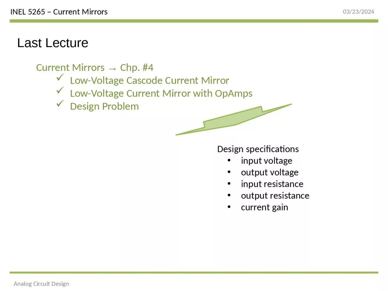
Last Lecture Current Mirrors Chp 4 LowVoltage Cascode Current Mirror LowVoltage Current Mirror with OpAmps Design Problem Design specifications input voltage output voltage ID: 1031053
Download Presentation The PPT/PDF document "9/2/2014 Analog Circuit Design" is the property of its rightful owner. Permission is granted to download and print the materials on this web site for personal, non-commercial use only, and to display it on your personal computer provided you do not modify the materials and that you retain all copyright notices contained in the materials. By downloading content from our website, you accept the terms of this agreement.


1. 9/2/2014Analog Circuit DesignLast LectureCurrent Mirrors → Chp. #4 Low-Voltage Cascode Current MirrorLow-Voltage Current Mirror with OpAmpsDesign ProblemDesign specifications input voltage output voltage input resistance output resistance current gain
2. 9/2/2014Analog Circuit Design2Problem #1 -bUsing the (W/L)s obtained part I, does de cascode current mirror still behaves properly for Rbias=40kΩ? Justify you answer.
3. 9/2/2014Analog Circuit Design3Problem #1 -cAssuming Ibias=10uA, and Vb=1.8V, design transistors M6-13 such that|Av|>30V/VOutput Voltage Range = 1.3V
4. 9/2/2014Analog Circuit Design4Problem #1 -dUsing the (W/L)s obtained on part III, find the possible voltage range for Vb such that the circuit still behaves properly.
5. 9/2/2014Analog Circuit Design5Homework #2Design the cascode current mirror for the following specifications:Iout = 2·Iin=[0-10] µAVout(min) < 0.5VVin < 0.9VM2=2·M1Vout(min)=Vds1(sat)+Vds2(sat) = 0.5VChoose Vds1(sat)=Vds2(sat)=0.25VFind W/L for M4,M2, and M1Vin(max)=Vgs1=Vton+Vds1(sat)=0.95Vdoes not satisfyVds1(sat)=0.2V in order to satisfyFind new W/L for M1 and M2Vgs3=Vgs4+Vds2(sat)Vds3(sat)=Vds4(sat)+Vds2(sat)=0.45VFind W/L for M3IbiasVDDM2M1IoutM4M3IinVout+_