
This might be in order to avoid the possibility of dangerous voltage s or currents from one half of the system doing damage in the other or to break an intract able ground loop Such a system is said to be isolated and the arrangement th at passes a ID: 29952
Download Pdf The PPT/PDF document "MT TUTORIAL Analog Isolation Amplifiers ..." is the property of its rightful owner. Permission is granted to download and print the materials on this web site for personal, non-commercial use only, and to display it on your personal computer provided you do not modify the materials and that you retain all copyright notices contained in the materials. By downloading content from our website, you accept the terms of this agreement.

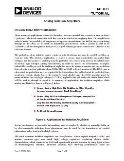
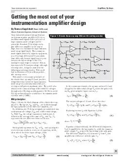


MT-071TUTORIAL Analog Isolation Amplifiers MT-071 sufficiently linear to pass high accuracy analog signals across an isolation barrier. With others, the signal may need to be converted to digital form before transmission for accuracy is to be maintained (note this is a common voltageTransformers are capable of analog accuracy of 12-16 bits and bandwidths up to several hundred kHz, but their maximum voltage rating rarely exceeds 10 kV, and is often much lower. isolation amplifiers have lower accuracy, perhaps 12-bits maximum, lower and can be made with very high voltage ratings (4more common ratings), but Linearity and isolation voltage are not the only issues to be considered in the choice of isolation systems. Operating power is of course, essential. Both the input and the output circuitry must be e isolation barrier (which is enient), some form of isolated power must be provided. Systems using transformer isolation can easily use a transformer (either the signal transformer or another one) to provide isolated power, but it is impractical to transmit useful amounts of power by capacitive or optical means. Systems using these forms of isolation must make other arrangements to obtain onsideration in favor of choosing transformer isolated isolation amplifiers: they almost iThe isolation amplifier has an i isolated from the power supply and the output circuit. In addition, there is minifor dc current flow, and minimum ac coupling. Isolation amplifiers are intended for applications requiring safe, accurate measurement of low frequency voltage or current (up to about 100 kHz) in the presence of high common-mode ith high common mode rejection. Threceiving of signals transmitted at high impedance in noisy environments, and for safety in general-purpose measurements, where dc and line-frequency leakage must be maintained at levels well below certain mandated minimums. Principal applications are in electrical environments of the kind associated with medical equipment,plants, automatic test equipment, and industrial process control systems. In a basic two-port form of isolator, the output not isolated from one (input, power, output) is shown in Figure 2 below. Note that in this diagram, the input circuits, output circuits, and ed from one another. This figure represents the circuit archite An isolator of this type requires power from a two-terminal dc power supply (PWR, PWR COM). An internal oscillator (50 kHz) converts h is transformer-coupled Page 2 of 6 MT-071 MOD DEMODFILTER DEMODFILTER +__+ SUPPLY OUTPUTSUPPLY OSCILLATOR INPUTOUTPUT+IN ISSPWRPWR COMCOM AD210 3-Port Isolation Amplifier by the input stage amplifier output, transformer-coupled to the output stage, demodulated by a phase-sensitive demodulator (using filtered, and buffered using isolated dc power derived from the carrier. The AD210 allows the user to select gains from sistors with the input section op amp. Bandwidth is 20 kHz, and voltage isolation is 2500 V rms (continuous) and 3500 V peak (continuous). The AD210 is a 3-port isolation amplifier, thus the power circuitry is isolated from both the input and the output stages and may therefore be conner (or to uses transformer isolation to achieve 3500 V Transformer CoupledHigh Common Mode Voltage Isolation:±3500V Peak ContinuousWide Bandwidth: 20kHz (Full Power)0.012% Maximum Linearity ErrorInput Amplifier: Gain 1 to 100Isolated Input and Output Power Supplies, ±15V, ±5mA Page 3 of 6 MT-071 MOTOR CONTROL ISOLATION AMPLIFIER APPLICATION A typical isolation amplifier application using the is shown in Figure 4 below. The AD210 is used with an AD620 instrumentation amplifier in a current-sensing system for motor can be directly connected to a 110 or 230 V ing necessary. The input section's isolated ±15 V powers the AD620, which senses the voltage drop in a smainput stage op amp is simply connected as a unity-gain follower, which minimizes its error contribution. The 110 or 230 V rms common-mode voltage is ignored by this isolated system. MOD DEMODFILTER DEMODFILTER +__+ INPUTSUPPLY POWER POWEROSCILLATOR OUTPUTPOWER–IN+IN ISSPWR COM OSS +15V–15V HIGH VOLAGEAC INPUT 2500V RMS 0.01AD620AD210 +15V FOR G = 100Figure 4: Motor Control Current Sensing Application Within this system the AD620 preamp is used asproduce and output voltage proportional to motor currand gain as set by the AD620's R. The AD620 also improves overall system accuracy, as the OS is 15 mV, versus the AD620's 30 µV (with less drift also). Note that if higher dc offset and drift are acceptable, the AD620 may be omitted and the AD210 connected at a gain of Due to the nature of this type of carrier-operated isolation system, there will be certain operating situations where some residual ac carrier component will be superimposed upon the recovered output dc signal. When this occurs, a low impedance passive RC filter section following the output stage may be used (if the following stage has a high input impedance, i.e., non-loading to be the case for many high input impedance sampling ADCs, which appear essentially as a small capacitor. A 150 resistance and 1 nF capacitor will provide a corner frequency of about 1 kHz. Note also that the capacitor should be a film type for low Page 4 of 6 MT-071 AD215 TWO-PORT ISOLATOR The AD215 is a high speed, two-port isolation amplifier, designed to isolate and amplify wide bandwidth analog signals. The innovative circuit and transformer design of the AD215 ensures wide-band dynamic characteristics, while preserving dc performance specifications. An AD215 AD215 Port Isolation Amplifier The AD215 provides complete galvcomplete design, powered by a ±15 V dc supply on the output side, eliminatessupplied isolated dc/dc converter. This permits the designer to minimize circuit overhead and reduce overall system design complexity and component costs. The design of the AD215 emphasizes maximum flexibapplications where fast analog signals must be measured under high common-mode voltage The AD215 has a ±10 V input/output range, a specified gain range of 1 V/V to 10 V/V, a buffered output with offset trim and a user-avaIsolation voltage: 1500V rmsFull power bandwidth: 120kHzSlew rate: 6V / µsHarmonic distortion: –80dB @ 1kHz0.005% maximum linearity errorGain range: 1 to 10Isolated input power supply: ±15V @ ±10mA Page 5 of 6 Page 6 of 6 REFERENCES Hank Zumbahlen, Basic Linear Design, Analog Devices, 2006, ISBN: 0-915550-28-1. Also available as Linear Circuit Design Handbook , Elsevier-Newnes, 2008, ISBN-10: 0750687037, ISBN-13: 978-0750687034. Chapter 2. Walter G. Jung, Op Amp Applications Analog Devices, 2002, ISBN 0-916550-26-5, Also available as Op Amp Applications Handbook , Elsevier/Newnes, 2005, ISBN 0-7506-7844-5. Chapter 2. Charles Kitchin and Lew Counts, A Designer's Guide to Instrumentation Amplifiers, 3 Edition , Analog Devices, 2006. Copyright 2009, Analog Devices, Inc. All rights reserved. Analog Devices assumes no responsibility for customer product design or the use or application of customers’ products or for any infringements of patents or rights of others which may result from Analog Devices assistance. All trademarks and logos are property of their respective holders. Information furnished by Analog Devices applications and development tools engineers is believed to be accurate and reliable, however no responsibility is assumed by Analog Devices regarding technical accuracy and topicality of the content provided in Analog Devices Tutorials.