/
1 Tunnel dielectric 1 Tunnel dielectric

1 Tunnel dielectric - PowerPoint Presentation

alexa-scheidler
alexa-scheidler . @alexa-scheidler
Follow
415 views
Uploaded On 2017-04-28

1 Tunnel dielectric - PPT Presentation

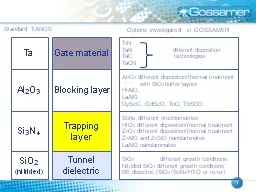
Trapping layer Blocking layer Gate material SiO 2 nitrided Si 3 N 4 Al 2 O 3 Ta Standard TANOS Options investigated in GOSSAMER SiO 2 different growth conditions Nitrided ID: 542576

sio2 cell deposition thermal cell sio2 thermal deposition array si3n4 effect device addressable channel charge nand growth sonos tanos

Share:

Link:

Embed:

Download Presentation from below link

Download Presentation The PPT/PDF document "1 Tunnel dielectric" is the property of its rightful owner. Permission is granted to download and print the materials on this web site for personal, non-commercial use only, and to display it on your personal computer provided you do not modify the materials and that you retain all copyright notices contained in the materials. By downloading content from our website, you accept the terms of this agreement.


Presentation Transcript

Slide1

1

Tunnel dielectric

Trapping layer

Blocking layer

Gate material

SiO

2(nitrided)

Si3N4

Al2O3

Ta

Standard TANOS

Options investigated in GOSSAMER

SiO2 different growth conditionsNitrided SiO2 different growth conditionsBE dielectric (SiO2 /Si3N4/HTO or re-ox)

Si3N4 different stochiometriesHfO2 different deposition/thermal treatmentZrO2 different deposition/thermal treatmentZrAlO and ZrSiO nanolaminatesLaAlO nanolaminates

Al2O3 different deposition/thermal treatment “ “ with SiO2 buffer layersHfAlO, LaAlODyScO, GdScO, TbO, TbSCO

TiNTaN different depositionTaC technologiesTaCNSlide2

2

1Gb TANOS demonstrator

Picture of 1Gbit NAND Charge Trap Flash

Numonyx inserted the Charge Trap cell into a 1Gbit 1.8V NAND device adapting cell pitch at row and column decoders thanks to an advanced copper

metallization

The device includes 1.8 billion cells but only 1 G is addressable due to the re-use of an existing cell design.

~40nm

500Mbit array

500Mbit array

RAM

Schematic layoutSlide3

22nm demonstration

3

In Self-Aligned structure, W narrowing increases P/E efficiency

Down to 1x nm node we estimate no significant degradation of P/E

windows

4Mbit addressable array at 25nm Slide4

4

3-D architectures

30nm

25nm

OXIDE

gate

- Effect of floating body channel

Effect of poly-silicon channel

Effect of wrap-around SONOS cellMulti-plane architecture

Vertical SONOS Cell(imec)

Program

v.s

. diameterprogramming voltage