PPT-1 ICC Proprietary
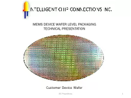
MEMS DEVICE WAFER LEVEL PACKAGING TECHNICAL PRESENTATION Customer Device Wafer Process Modification Required as follows Reduction of Bond pads to half of existing
Download Presentation
"1 ICC Proprietary" is the property of its rightful owner. Permission is granted to download and print materials on this website for personal, non-commercial use only, provided you retain all copyright notices. By downloading content from our website, you accept the terms of this agreement.
Presentation Transcript
Transcript not available.