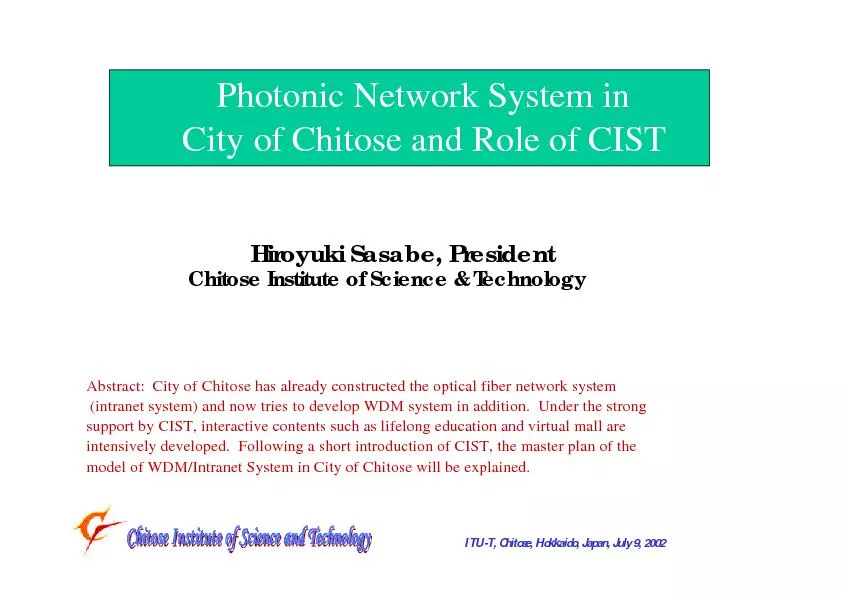
/
PhotonicNetwork System in City ofChitoseand Role of CIST PhotonicNetwork System in City ofChitoseand Role of CIST

PhotonicNetwork System in City ofChitoseand Role of CIST - PDF document

briana-ranney
briana-ranney . @briana-ranney
Follow
374 views
Uploaded On 2016-05-20

PhotonicNetwork System in City ofChitoseand Role of CIST - PPT Presentation

Major Projects inChitose Chitose Industrial Complex Chitose Science ParkNew Chitose AirportCISTChitose Bibi WorldChitose Office Arcadia Chitose Delivery ComplexChitose Industrial Complex JR Minami JR ID: 327812

Major Projects inChitose Chitose Industrial Complex Chitose

Share:

Link:

Embed:

Download Presentation from below link

Download Pdf The PPT/PDF document "PhotonicNetwork System in City ofChitose..." is the property of its rightful owner. Permission is granted to download and print the materials on this web site for personal, non-commercial use only, and to display it on your personal computer provided you do not modify the materials and that you retain all copyright notices contained in the materials. By downloading content from our website, you accept the terms of this agreement.


Presentation Transcript

PhotonicNetwork System in City ofChitoseand Role of CIST Major Projects inChitose Chitose Industrial Complex Chitose Science ParkNew Chitose AirportCISTChitose Bibi WorldChitose Office Arcadia Chitose Delivery ComplexChitose Industrial Complex JR Minami JR ChitoseTo: SapporoTo: Tomakomai JR Osatsu Scheme of Photonics Valley Project Started in 1995 Scheme of Photonics Valley Project Photonics World Consortium (PWC)Collaborative CoordinationTechnological CoordinationTechnology Transfer of Fundamental ResearchesChitose Institute of Science & Technology (CIST)Graduate School of CISTFundamental/ Practical ResearchesHuman Resource DevelopmentIntellectual AccumulationHuman and Intellectual Interaction betweenAcademia and Industry Chitose Institute of Science & Technology (CIST) History of CIST Foundation: April 1, 19981 Faculty (PhotonicsScience and Technology) 2 Departments:PhotonicsMaterials ScienceApplied Photonics System Technology1President Prof. Keisuke Sasaki (April 1998 –Oct 1998)2President Prof. Naoya Ogata (Nov 1998 –March 2002)3President Prof. Hiroyuki Sasabe (April 2002 –to date)Graduate School: April 1, 20021 Department (Photonics Science and Technology)1Dean Prof. Hiroyuki Sasabe (April 2002 –to date) International Meetings ICONO4 (4thInternational Conference on Organic Nonlinear Optics)Oct 12 –14, 1998CIF1 (1stChitose International Forum on Organic PhotonicsOct 6-8, 1999ISOM 2000 (International Symposium on Optical Memories 2000)Sept 5-8, 2000CIF2 (2ndChitose International Forum on Organic PhotonicsSept 6-9, 2001CIF3 (3rdInternational Forum on Organic PhotonicsOct 6-9, 2002 Photonics World Consortium (PWC) Foundation : August 28, 1997 as a private organizationJune 6, 2001 approved as a non-profitable organization (NPO)(under the ‘Photonics Valley Project’promoted by the City of ChitoseObjectives : Formation of worldwide R&D Base on photonics sci & tech ·Development of organic optoelectronic materials and devices foropitcal communications, photonic network systems, etc ·Base for intimate collaboration among academia, industry and local government ·Human resource development, technological innovation towardapplication, and formation of human networks in the field of President: Prof. H. Sasabe (CIST) (June 2002 - Research Cluster Activities in PWC Biophotonics Research ClusterThis cluster aims Primarily at the basic understandings of what is biophotonics and how to develop biophotonics through the literature survey, and then seeks the target programs available in the local area of Hokkaido. One of the promising targets is the medical diagnostics and therapy using photodynamic techniques, and the other the agricultural applications using photogenetic modification of plants. Under these activities we will form a consortium to propose a national project on biophotonics to the Government.Cluster Coordinator: Hiroyuki Sasabe ( CIST ) 1966Master of Engineering, University of Tokyo, Applied Physics 1972Doctor of Engineering, University of Tokyo 1966Electrotechnical Laboratory, AIST, MITI 1974Associate Professor, Tokyo University of Agriculture & Technology, Dept. Electronic Eng., 1983Chief Scientist, The Institute of Physical and Chemical Research(RIKEN ) 1999Professor, Chitose Institute of Science & Technology ( CIST ), Dept. Photonics Materials SciPresident of CIST, Dean of CIST Graduate School Organic Semiconductor DevicesResearch clusterThe research objective is for exploring a new electronic world, organic electronics ( OE ). Since the 1980’s, the progress of organic semiconductors in both low molecular materials and polymers are expanding due to the unique electronic properties as unlike as inorganic semiconductors, leading to novel optoelectronic applications. We will focus on electronic and optical properties of organic semiconductors which open novel optoelectronic applications. Through discussion and investigation of previous papers, we explore new organic device applications and develop the device performances. Furthermore, we’d like to establish device physics of organic semiconductors.Cluster Coordinator: Chihaya Adachi ( CIST )1991.3Doctor of Engineering, Kyushu University 1991.4Ricoh Co.Ltd., Chemical Products R&D Center 1996.8Research Associate, Shinshu University, Department of FunctionalPolymer Science 1999.5Research Staff, Department of Electrical Engineering, Princeton University, USA 2001.7Associate Professor, Department of Photonics Materials Science, CIST Research Cluster Activities in PWC Organic NanoResearch ClusterNanotechnology is an integral part of photonics science and technology. For various applications in the field of photonics and electronics it is necessary to control the nanoscopic structure of organic molecules, their orientation, and aggregation.Nanotechnology can offer various ways to achieve the goals of highly functionalnovel device. For example, the self-assembly of molecules offers the possibility to pattern molecules on the molecular level, something that is difficult for the common technique of lithography. The Nanotech Cluster will bridge the gap between the present state-art science and possible future applications and will offer seeds for future applications of nanotech devices.Cluster Coordinator: Olaf Karthaus (CIST ) Diploma Degree from the Faculty of Chemistry of the Johannes Gutenberg University, Mainz, Germany1992Doctor Degree (Dr.rer) from the Faculty of Chemistry and Pharmacy of the Johannes Gutenberg University, Mainz, Germany1992JSPS and Alexander-Humboldt fellowship at the Faculty ofEngineering of Tohoku University, Sendai, Japan1994Research Associate at the Research Institute for Electronic Science,Hokkaido University, Sapporo, Japan2000Associate Professor, Chitose Institute of Science and Technology Photonic networks and broadband access systemsThis cluster studies research and development trend or directionof recent photonic systems, such as photonic networks and broadband access networks, which lead innovation oftraditional communication networks. Also it discusses novel devices, components, and sub-systems for such advanced networks or systems from the viewpoint of market needs and find buisness opportunities.The cluster is planning various kinds of activities, such as meetings, lectures, forums, and publishing reports, etc., during the fiscal year 2002.Cluster Coordinator: Masaaki Kawase( CIST ) 1972Master of Engineering, Hokkaido University, electrical engineering1991Doctor of Engineering, Hokkaido University1972NTT Laboratories 1999Professor, Chitose Institute of Science & Technology ( CIST ) Research Cluster Activities in PWC Ultrafastand Broadband Optical Technology and Its Applications ClusterUltrafastand broadband optical technology is applied in not only opticalcommunication technology, but in chemistry, biology, nanoand many other fields. In this cluster, we try to apply ultrashortoptical pulse technology in various fields and to propose novelfunctions, techniques, devices and system that utilize temporal, spectral, spatial, coherent and characteristics ofultrashortoptical pulses.Cluster Coordinator: Mikio (Hokkaido University) 1970Master of Engineering, Department of Electronics Engineering,Kyoto University1976 Doctor of Engineering, Department of Electronics Engineering,Kyoto University1970 ElectrontechnicalLaboratory, AIST, MITI1978 Imperial College, University of London1991 Professor, Department of Engineering Science, Hokkaido University Professor, Department of Applied Physics, Hokkaido University Development of Phonic Network and New Web Application System ClusterTechnologies for the phonic network and new web application system are studied in this cluster. Market research and forum will be held among this group. Active people are strongly welcome to create new technology. One of the important subjects is high speed access area network system (photonic network system) using plastic optical fibers (POF), and the research about new materials, devices, integrated systems is carried out.Cluster Coordinator: Suguru Horinouchi( CIST ) 19911993 Keio University (Master Course): Development of fiber optics19931996 Keio University (Doctor Course): Development of fiber optics19961998 Visiting Researcher of Keio University19982001 Telecommunication Advancement Organization (Government Project) Project sub-now Lecturer ofChitoseInstitute of Science and Technology2001now President of Gootech -Multimedia Pilot Town Project-from 1998 Construction of the regional information database and systemDigital Library including 15,000 pages of historical data in ChitoseVirtual University and Library in which users can walk through CIST and the city library. Distance Learning including the memorial lectures in CISTELearning including 1,000 materials and exercises of mathematics for the junior, the high school and the college students. by Prof. Komatsugawa Nw Stfrom 2001 Field Test Collaborated with Chitose CitizenLearning System is not only used in junior high schools ofChitosebut widely used in Hokkaido area. Virtual Market Place is starting with the Local Chamber of Commerce of Chitose by Prof.Komatsugawa Intranet Systems in Chitose in FY2000-Information NW Center InternetBureau of Water SupplyJunior High SchoolsArt and Culture CenterChitose Inst. Sci. & TechJunior High SchoolsLibraryCity HallWelfare CenterArcadia PlazaElementary SchoolsEducation CommitteeFire HousesGovernment Office Metropolitan HospitalGallery Lifelong Learning Systems Government InformationSystemsEducation Support Systems Clean Center Optical Fiber100 Indoor Pool Community CentersSalmon ParkDone in 2002 Food Supply Center Optical Fiber100 Fire Department Optical Fiber100 Community CenterPublic HallElementary SchoolsCompaniesTotal Length 41 kmCost 4 M$ NPhysical Topology of the STAR WDM networkwith N wavelengthsLogical Topology ofNxNfull mesh networkOther networksWDM Bridgel,..., l Trial: AWGSTAR Network AWGSTAR is a WDM network which routes signals based on wavelength (wavelength routing results in the creation of a wavelength path) (C)2002 NTT Fiber optic intranet Subnet for video processing(Local Address) Sub(Global Address) WDM interface WDM TV camera meshEditing/control centerIVideo editingVideo editingVideo editingVideo editingVideo editingVideo editing WDM interface Network Structure AWG (C)2002 NTT Broad Band Access NW Ubiquitousbased Local Community Broad Band Access NW MultiAgent SystemsPhotonic Network D Virtual MallSystem Lifelong LearningLocal CommunityDatabaseLocal CommunitySystem Support System Lifelong LearningSystem Interactive Contents Wireless LAN Citizens Large Capacity Delivery ofHigh QualityMedia Single Sign-on Platform for Decentralized Authentication Systems Commerce Social CommunityBusiness Community Information Internal Currency(EcoKnowledge Database Test Bed for Ubiquitous-based Local Community MIND in Chitose 21 l Node 1 l Node nl, l2, .., l, l2, .., l . … . N x N Cyclic-Frequency AWGl, l2, .., l, l2, .., l2 . … . 2 Basic operation of wavelength routing for cyclic frequency AWG (C)2002 NTT 72 nodes5 x 5 in FY2002