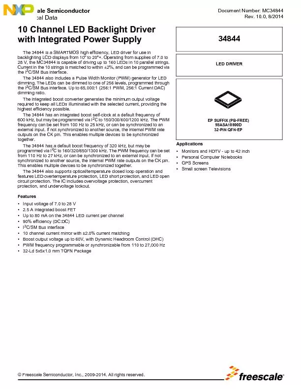
/
Document Number: MC34844Rev. 10.0, 8/2014Technical Data Document Number: MC34844Rev. 10.0, 8/2014Technical Data

Document Number: MC34844Rev. 10.0, 8/2014Technical Data - PDF document

calandra-battersby
calandra-battersby . @calandra-battersby
Follow
401 views
Uploaded On 2016-10-28

Document Number: MC34844Rev. 10.0, 8/2014Technical Data - PPT Presentation

10 Channel LED Backlight Driver with Integrated Power Supply The 34844 is a SMARTMOS high efficiency LED driver for use in backlighting LCD displays from 10 to 20 Operating from supplies of 70 ID: 481635

Channel LED Backlight Driver

Share:

Link:

Embed:

Download Presentation from below link

Download Pdf The PPT/PDF document "Document Number: MC34844Rev. 10.0, 8/201..." is the property of its rightful owner. Permission is granted to download and print the materials on this web site for personal, non-commercial use only, and to display it on your personal computer provided you do not modify the materials and that you retain all copyright notices contained in the materials. By downloading content from our website, you accept the terms of this agreement.


Presentation Transcript

Document Number: MC34844Rev. 10.0, 8/2014Technical Data© Freescale Semiconductor, Inc., 2009-2014. All rights reserved. 10 Channel LED Backlight Driver with Integrated Power Supply The 34844 is a SMARTMOS high efficiency, LED driver for use in backlighting LCD displays from 10" to 20"+. Operating from supplies of 7.0 to V, the MC34844 is capable of driving up to 160 LEDs in 10 parallel strings. Current in the 10 strings is matched to within 2%, and can be programmed via the I C/SM Bus interface. The 34844 also includes a Pulse Width Monitor (PWM) generator for LED dimming. The LEDs can be dimmed to one of 256 levels, programmed through the I 2 C/SM Bus interface. Up to 65,000:1 (256:1 PWM, 256:1 Current DAC) The integrated boost converter generates the minimum output voltage required to keep all LEDs illuminated with the selected current, providing the highest efficiency possible. The 34844 has an integrated boost self-clock at a default frequency of kHz, but may be programmed via I 2 C to 150/300/600/1200 kHz. The PWM frequency can be set from 100 Hz to 25 kHz, or can be synchronized to an external input. If not synchronized to another source, the internal PWM rate The 34844 has a default boost frequency of 320 kHz, but may be programmed via I 2 C to 160/320/650/1300 kHz. The PWM frequency can be set from 110 Hz to 27 kHz, or can be synchronized to an external input. If not synchronized to another source, the internal PWM rate outputs on the CK pin. This enables multiple devices to be synchronized together. The 34844 also supports optical/temperature closed loop operation and features LED overtemperature protection, LED short protection, and LED open circuit protection. The IC includes overvoltage protection, overcurrent protection, and undervoltage lockout. Features •Input voltage of 7.0 to 28 V •2.5 A integrated boost FET •Up to 80 mA on the 34844 LED current per channel •90% efficiency (DC:DC) •I C/SM Bus interface •10 channel current mirror with ±2.0% current matching •Boost output voltage up to 60V, with Dynamic Headroom Control (DHC) •PWM frequency programmable or synchronizable from 110 to 27,000 •32-Ld 5x5x1.0 mm TQFN Package 98ASA10800D32-PIN QFN-EPApplications•Monitors and HDTV - up to 42 inch•Personal Computer Notebooks Analog Integrated Circuit Device Data Figure 1. MC34844 Simplified Application Diagram (SM Bus Mode) Figure 2. MC34844 Simplified Application Diagram (Manual Mode) 7.0 to 28V FAILPGNDA34844PGNDB I1I2I4I5 I8 VCC GNDSCKSDAA0/SENISETVDC1VDC2VDC3COMPSLOPEPWM Control Unit M/~S VDC1 VDC1 ~~~~~~~~~~~~~~~~~~~ VDC1 7.0 to 28V 34844 I1I2I3I6I7 I8 VCC A0/SENISETCOMPSLOPE Control Unit M/~S VDC1 ~~~~~~~~~~~~~~~~~~~ VOUT PWM PWM VDC1VDC2VDC3 Analog Integrated Circuit Device DataFreescale Semiconductor ORDERABLE PARTS ORDERABLE PARTS This section describes the part numbers available to be purchased along with their differences. Valid orderable part numbers are provided on the web. To determine the orderable part numbers for this device, go to http://www.freescale.com and perform a part number search for the following device numbers.Table 1. Orderable Part Variations Part Number Notes Temperature (T PackageMC34844AEP(1)-40 to 105 °C32 QFN-EP1.To order parts in Tape & Reel, add the R2 suffix to the part number. Analog Integrated Circuit Device Data INTERNAL BLOCK DIAGRAM INTERNAL BLOCK DIAGRAM Figure 3. 34844 Simplified Internal Block Diagram COMPSWASWBPGNDATEMP/OPTOCURRENT DACOCP/OTP/UVLO10 CHANNEL CONTROLLER 80mA CURRENTMIRROR V SENSE GND A0/SENPGNDB LDO VDC2 SLOPE C INTERFACE VOUT Analog Integrated Circuit Device DataFreescale Semiconductor PIN CONNECTIONS PIN CONNECTIONS Figure 4. 34844 Pin Connections A functional description of each pin can be found in the Functional Pin Description section beginning on page Table 2. 34844 Pin Definitions Pin Number Pin Name Pin Function Formal Name Definition VIN Input voltage Input supply 2 PGNDB Power Power Ground Power ground 3 Switch node B Boost switch connection B 4 Switch node A Boost switch connection A 5 PGNDA Power Power Ground Power ground 6 A0/SEN Device Select Address select, device select pin or OVP HW control 7 Enable pin (active high, internal pull-up) 8 - 17 I0-I9 LED Channel LED string connections 18 Open Drain Fault detection Fault detected pin (open drain): No Failure = low-impedance Failure = high-impedance 19 ISET Passive Current set LED current setting resistor 20 PIN Positive current scale Positive input analog current control 21 Negative current scale Negative input analog current control Passive Boost Slope Boost slope compensation setting resistor 23 Internal Regulator 3 Decoupling capacitor for internal phase locked loop power 24 Clock signal Clock synchronization pin (input for M/~S = low - internal pull-up, output for = PWM External PWM External PWM input (internal pull-down) SWBSWASLOPEISETI1I2I3I4I5I6I7I8323130292827269101112131415QFN - EP5MM X 5MM32 LEADEP GNDEP = Exposed PadTransparent Top View Analog Integrated Circuit Device Data PIN CONNECTIONS Bidirectional 2 C data I 2 C data line 27 Bidirectional 2 C clock I 2 C clock line 28 Internal Regulator 1 Decoupling capacitor for internal logic rail 29 Passive Compensation pin Boost converter typecompensation pin 30 Master/Slave selector Selects Master mode (1) or Slave mode (0) Internal Regulator 2 Decoupling capacitor for internal regulator 32 VOUT Voltage Output Boost output voltage sense pin EP Ground reference for all internal circuits other than boost FET Table 2. 34844 Pin Definitions (continued)Pin NumberPin NamePin FunctionFormal NameDefinition Analog Integrated Circuit Device DataFreescale Semiconductor ELECTRICAL CHARACTERISTICSMAXIMUM RATINGS ELECTRICAL CHARACTERISTICS MAXIMUM RATINGS Table 3. Maximum Ratings All voltages are with respect to ground unless otherwise noted. Exceeding these ratings may cause a malfunction or permanent da Symbol Ratings Unit Notes ELECTRICAL RATINGS V MAX Maximum Pin Voltages A0/SEN I0, I1, I2, I3, I4, I5, I6, I7, I8, I9 EN, VIN SWA, SWB, VOUT FAIL, PIN, NIN, ISET, M/~S, CK, PWM 7.0 30 65 (5) MAX Maximum LED Current 85 ESD Voltage Human Body Model (HBM) Machine Model (MM) + (2) THERMAL RATINGS T A Ambient Temperature Range -40 to 105 °C Junction to Ambient Temperature 32 °C/W (3) Junction to Case Temperature 3.5 °C/W (3) J Maximum junction temperature 150 TSTO Storage temperature range -40 to 150 °C Peak Package Reflow Temperature During Reflow (4) Power Dissipation TA = 25 TA = 70 TA = 85 TA = 105 2.5 2.0 1.4 Notes 2.ESD testing is performed in accordance with the Human Body Model (HBM) (AEC-Q100-2), and the Machine Model (MM) (AEC-Q100-003 R = 0 3.Per JEDEC51 Standard for Multilayer PCB 4.Pin soldering temperature limit is for 10 seconds maximum duration. Not designed for immersion soldering. Exceeding these limits may cause malfunction or permanent damage to the device. 5.45 V is the Maximum allowable voltage on all LED channels in off-state. Analog Integrated Circuit Device Data ELECTRICAL CHARACTERISTICSSTATIC AND DYNAMIC ELECTRICAL CHARACTERISTICS STATIC AND DYNAMIC ELECTRICAL CHARACTERISTICS Table 4. Static and Dynamic Electrical Characteristics Characteristics noted under conditions V IN = 12 V, V OUT = 42 V, PWM = VDC1, M/~S = VDC1, PIN & NIN = VDC1, -40 105 C, PGND = 0 V, unless otherwise noted. Symbol Characteristic Typ Unit Notes 7.0 28 (8) SHUTDOWN Supply Current when Shutdown Mode Manual: PWM = Low, EN = Low, SCK & SDA=Low SM Bus: EN bit = 0, SCK & SDA=Low, EN pin= Low I 2 C: SETI2Cbit=1, CLRI2C=0, EN bit= 0, EN pin = Low - - - A I SLEEP Supply Current when Sleep Mode SM-Bus: EN = low, SCK & SDA = Active, SETI2C bit = 0, EN bit = 0 I 2 C: EN = High, SETI 2 C bit = 1, CLRI 2 C bit = 0, EN bit = 0 - Supply Current when Operational Mode Manual: EN = High, SCK & SDA =Low, PWM = Low, SM-Bus: EN = Low, SCK & SDA = Active, EN bit = 1, PWM = Low I 2 C: EN = High, SETI 2 C bit = 1, CLRI 2 C bit = 0, EN bit = 1, PWM = Undervoltage Lockout (V IN Rising) 5.4 6.0 6.4 Undervoltage Hysteresis (V IN Falling) - DC1 VDC1 Voltage C = 2.2 F 2.5 2.75 (6) DC2 VDC2 Voltage C = 2.2 F 6.0 6.5 (6) DC3 VDC3 Voltage C = 2.2 F 2.5 2.75 (6) BOOST Output Voltage Range VIN = 7.0 V VIN = 28 V - 60 (7) (8) Boost Switch Current Limit 2.3 2.5 2.7 t Boost Switch Current Limit Timeout - DS(ON) of Internal FET (I DRAIN = 1.0 A)( 500 BOOST_LEAK Boost Switch Off-state Leakage Current V SWA,SWB = 65 V Feedback pin Off-state Leakage Current (V OUT = 65 V ) BOOST Peak Boost Efficiency - (8) Line Regulation - VIN = 7.0 to 28 V %/V (8) Load Regulation - VLED = 8.0 to 65 V (all Channels) -0.2 %/V (8) Notes 6.This output is for internal use only and not to be used for other purposes. A 1.0 resistor between the VDC3 and VDC1 pin is recommended for °C operation. 7.Minimum and Maximum output voltages are dependent on Min/Max duty cycle and current limit condition. 8.Guaranteed by design Analog Integrated Circuit Device DataFreescale Semiconductor ELECTRICAL CHARACTERISTICSSTATIC AND DYNAMIC ELECTRICAL CHARACTERISTICS BOOST (CONTINUED) V SLOPE Slope compensation voltage ramp - R SLOPE = 68 k s Current Sense Amplifier Gain - Current Sense Resistor - M OTA Transconductance - S Transconductance Sink and Source Current Capability - A FAIL PIN I FAIL_LEAK Off-state Leakage Current - V FAIL = 5.5 V - - A On-state Voltage Drop - I = 4.0 LED CHANNELS I SINK Sink Current ICHx Register = 255, PIN&NIN = Disabled, T A  78.4 V Regulated minimum voltage across 625 775 Current Matching Accuracy -2.0 V SET Pin Voltage RISET=3.48  2.048 LED Current Amplitude Resolution 1.0 80 % I CH_LEAK Off-state Leakage Current, All channels - (V CH = 45 - A PIN INPUT V PIN_DIS Voltage to Disable PIN mode 2.2 - V I PIN Bias Current PIN = V SET A I DIM_PIN Analog Dimming Current, ICHx Register = 255, RISET=3.48 0.1% PIN = V SET PIN = V SET 76 80 44 84 NIN INPUT V NIN_DIS Voltage to Disable NIN mode 2.2 - V I NIN Bias Current NIN = V SET A I DIM_NIN Analog Dimming Current ICHx Register = 255, RISET=3.48 0.1% NIN = V SET /2 NIN = 0 V 36 76 80 44 84 Table 4. Static and Dynamic Electrical Characteristics (continued)Characteristics noted under conditions VIN = 12 V, VOUT = 42 V, PWM = VDC1, M/~S = VDC1, PIN & NIN = VDC1, -40 105PGND = 0 V, unless otherwise noted. Symbol Characteristic Typ Unit Notes Analog Integrated Circuit Device Data ELECTRICAL CHARACTERISTICSSTATIC AND DYNAMIC ELECTRICAL CHARACTERISTICS OVER-TEMPERATURE PROTECTION O Over-temperature Threshold Rising Hysteresis 150 25 175 (9) 2 C/SM BUS PHYSICAL LAYER [SCK, SDA] ADR 2 C Address - Binary ADR SM-Bus Address - Binary ILI Input Low Voltage -0.3 V Input High Voltage 2.1 Input Hysteresis - Output Low Voltage Sink Current 4.0 - I Input Current -5.0 A INI Input Capacitance F (9) LOGIC INPUTS / OUTPUTS (CK, M/~S, PWM, A0/SEN, EN) V Input Low Voltage -0.3 V Input High Voltage 1.5 Input Hysteresis - Input Low Voltage (EN) -0.3 V Input High Voltage (EN) 2.1 V Output Low Voltage (CK) I 2.0 - V OHL Output High Voltage (CK) I 2.0 Input Current -5.0 A INI Input Capacitance F (9) OVER-VOLTAGE PROTECTION Over-voltage Clamp - OVP Register Table: OVP OVP = Fh (Default) 60.5 62.5 64.5 OVP = Eh 56.5 60 OVP = Dh 53 56 OVP = Ch 49 OVP = Bh 45 OVP = Ah 41 OVP OVP = 9h 38 OVP OVP = 8h 34 OVP OVP = 7h 30.5 Notes 9.Guaranteed by design Table 4. Static and Dynamic Electrical Characteristics (continued)Characteristics noted under conditions VIN = 12 V, VOUT = 42 V, PWM = VDC1, M/~S = VDC1, PIN & NIN = VDC1, -40 105PGND = 0 V, unless otherwise noted. Symbol Characteristic Typ Unit Notes Analog Integrated Circuit Device DataFreescale Semiconductor ELECTRICAL CHARACTERISTICSSTATIC AND DYNAMIC ELECTRICAL CHARACTERISTICS OVER-VOLTAGE PROTECTION (CONTINUED) Over-voltage Clamp - OVP Register Table: OVP OVP = 6h 26 30 OVP OVP = 5h 23 25 Over-voltage threshold, Set by Hardware, Voltage at A0/SEN 6.15 6.5 6.85 I SINK_OVP A0/SEN Sink Current, T 130 A Switching Frequency (BST [1:0]=0) 0.14 Switching Frequency (BST [1:0]=1) (Default) 0.29 Switching Frequency (BST [1:0]=2) 0.59 Switching Frequency (BST [1:0]=3) 1.17 Boost Switching Frequency 0.29 Minimum Duty Cycle - 15 D Maximum Duty Cycle 80 % Soft Start Period - Boost Switch Rise Time - (10) F Boost Switch Fall Time - (10) PWM GENERATOR fPWM PWM Frequency Range M/~S = Low (Slave Mode) 110 (10) PWM Frequency, M/~S = High (Master Mode) FPWM Register = 768 FPWM Register = 192,000 25000 103 110 112 fPWM PWM dimming resolution - % T PWM CONTROL) t PWM_IN Input PWM Pin Minimum Pulse 150 (10) Input PWM Frequency Range 110 PHASE LOCK LOOP fCK S CK Slave Mode Frequency Lock Range, M/~S = Low (Slave Mode) 110 (11) S_JITTER CK Slave Mode Input Jitter, M/~S = Low (Slave Mode) - (10) Slave Mode Acquisition Time, M/~S = Low (Slave Mode) FPWM FPWM - 2000 - MASTER CK Frequency (Master Mode) FPWM Register = 768 FPWM Register = 192,000 25000 103 110 112 Notes 10.Guaranteed by design 11.Special considerations should be made for frequencies between 110 Hz to 1.0 KHz. Please refer to Functional Device Operation for further details. Table 4. Static and Dynamic Electrical Characteristics (continued)Characteristics noted under conditions VIN = 12 V, VOUT = 42 V, PWM = VDC1, M/~S = VDC1, PIN & NIN = VDC1, -40 105PGND = 0 V, unless otherwise noted. Symbol Characteristic Typ Unit Notes Analog Integrated Circuit Device Data ELECTRICAL CHARACTERISTICSSTATIC AND DYNAMIC ELECTRICAL CHARACTERISTICS I 2 C/SM BUS PHYSICAL LAYER [SCK, SDA] f Interface Frequency Range 400 kHz SM Bus Power-on-Reset Time - SHUTDOWN SM Bus Shut down mode Timeout - F Output fall time 10 F (12) R Output rise time 10 F C L F (12) LOGIC OUTPUT (CK) t R Output Rise and Fall time L F LED CHANNELS t R Channels Rise and Fall Time - (12) Notes 12.Guaranteed by design Table 4. Static and Dynamic Electrical Characteristics (continued)Characteristics noted under conditions VIN = 12 V, VOUT = 42 V, PWM = VDC1, M/~S = VDC1, PIN & NIN = VDC1, -40 105PGND = 0 V, unless otherwise noted. Symbol Characteristic Typ Unit Notes Analog Integrated Circuit Device DataFreescale Semiconductor FUNCTIONAL DESCRIPTIONINTRODUCTION FUNCTIONAL DESCRIPTION INTRODUCTION LED backlighting is very popular for small and medium LCDs, due to some advantages over other backlighting schemes, such as thewidely used cold cathode fluorescent lamp (CCFL). The advantages of LED backlighting are low cost, long life, immunity to vibration, low operational voltage, and precise control over its intensity. However, there is an important drawback of this method. It requires more power than most of the other methods, and this is a major problem if the LCD size is large enough. To address the power consumption problem, solid state optoelectronics technologies are evolving to create brighter LEDs with lopower consumption. These new technologies together with highly efficient power management LED drivers are turning LEDs, a more suitable solution for backlighting of almost any size of LCD panel, with really conservative power consumption. One of the most common schemes for backlighting with LED is the one known as “Array backlighting”. This creates a matrix of LEDall over the LCD surface, using defraction and diffused layers to produce an homogenous and even light at the LCD surface. Each row or column is formed by a number of LEDs in series, forcing a single current to flow through all LEDs in each string. Using a current control driver, per row or column, helps the system to maintain a constant current flowing through each line, keeping a steady amount of light even with the presence of line or load variations. They can also be use as a light intensity control by increasing or decreasing the amount of current flowing through each LED string. To achieve enough voltage to drive a number of LEDs in series, a boost converter is implemented to produce a higher voltage frosmaller one, which is typically used by the logical blocks to do their function. The 34844 implements a single channel boost converter together with 10 input channels, for driving up to 16 LEDs per string to create a matrix of more than 160 LEDs. Together with iefficiency and I 2 C programmable or external current control, among other features, makes the 34844 a perfect solution for backlighting small and medium size LCD panels, on low power portable and high definition devices. FUNCTIONAL PIN DESCRIPTION INPUT VOLTAGE SUPPLY (VIN) IC Power input supply voltage, is used internally to produce internal voltage regulation (VDC1, VDC3) for logic functioning, and also as an input voltage for the boost regulator. INTERNAL VOLTAGE REGULATOR 1 (VDC1) This pin is for internal use only, and not to be used for other purposes. A capacitor of 2.2 F should be connected between this pin and ground for decoupling purposes. INTERNAL VOLTAGE REGULATOR 2 (VDC2) This pin is for internal use only, and not to be used for other purposes. A capacitor of 2.2 F should be connected between this pin and ground for decoupling purposes. INTERNAL VOLTAGE REGULATOR 3 (VDC3) This pin is for internal use only, and not to be used for other purposes. A capacitor of 2.2 F should be connected between this pin and ground for decoupling purposes. A 1.0 resistor between the VDC3 and VDC1 pin is recommended for -20 °C operation. BOOST COMPENSATION PIN (COMP) Passive terminal used to compensate the boost converter. Add a capacitor and a resistor in series to GND to stabilize the syste IC ENABLE (EN) The active high enable terminal is internally pulled high through pull-up resistors. Applying 0V to this terminal would stop the IC from working. INPUT/OUTPUT CLOCK SIGNAL (CK) This terminal can be used as an output clock signal (master mode), or input clock signal (slave mode), to synchronize more than one device. MASTER/SLAVE MODE Setting this pin high puts the device into Master mode, producing an output synchronization clock at the CK terminal. Setting this pin low, puts the device in Slave mode, using the CK pin as an input clock. Analog Integrated Circuit Device Data FUNCTIONAL DESCRIPTIONFUNCTIONAL PIN DESCRIPTION EXTERNAL PWM INPUT (PWM) This terminal is internally pulled down. An external PWM signal can be applied to modulate the LED channel directly in absence of an 2 C interface. CLOCK I 2 C SIGNAL (SCK) Clock line for I 2 C communication. ADDRESS I 2 C SIGNAL (SDA) Address line for I 2 C communication. A0/SEN Address select, device select pin, or hardware overvoltage protection (OVP) control. CURRENT SET (ISET) Each LED string can drive up to 50 mA. The maximum current can be set by using a resistor from this pin to GND. POSITIVE CURRENT SCALING (PIN) Positive current scaling factor for the external analog current control. Applying 0 V to this pin, scales the current to near 0%, and in the same way, applying V SET (2.048 V Typ.), the scale factor is 100%. By applying a voltage higher than 2.2 V, the scaling factor is disabled, and the internal pull-ups are activated. If PIN pin and NIN pin are used at the same time then by applying 0 V to the PIN pin and V SET to NIN pin, scales the current to near 0%, and in the same way, applying V SET to the PIN pin and 0 V to NIN pin, scales the current to 100%. By applying a voltage higher than V, the scaling factor is disabled and the internal pull-ups are activated in both pins. NEGATIVE CURRENT SCALING (NIN) Negative current scaling factor for the external analog current control. Setting 0 V to this pin scales the current to 100%, in the same SET (2.048 V Typ.) the scale factor is near 0%. By applying a voltage higher than 2.2 V, the scaling factor is disabled and the internal pull-ups are activated. If the PIN and NIN pin are used at the same time, then by applying 0 V to the PIN pin and V SET to NIN pin, it scales the current to near 0%, and in the same way, applying V SET to the PIN pin and 0 V to NIN pin, scales the current to 100%. By applying a voltage higher than V, the scaling factor is disabled and the internal pull-ups are activated in both pins. GROUND (GND) Ground Reference for all internal circuits other than the Boost FET. The Exposed Pad (EP) should be used for thermal heat dissipation. Current LED driver, each line has the capability of driving up to 50 mA. FAULT DETECTION PIN (FAIL) When a fault situation is detected, this pin goes into high-impedance. BOOST SLOPE COMPENSATION SETTING RESISTOR (SLOPE) The resistor to be used for the SLOPE depends on the Input and Output voltage difference as well as the inductor value. Use the formula shown in the Components Calculation section to calculate the value accordingly. POWER GROUND TERMINALS (PGNDA, PGNDB) Ground terminal for the internal Boost FET. OUTPUT VOLTAGE SENSE TERMINAL (VOUT) Input terminal to monitor the output voltage. It supplies the input voltage for the internal regulator 2 (VDC2). SWITCHING NODE TERMINALS (SWA, SWB) Switching node of boost converter. Analog Integrated Circuit Device DataFreescale Semiconductor FUNCTIONAL DESCRIPTIONFUNCTIONAL INTERNAL BLOCK DESCRIPTION FUNCTIONAL INTERNAL BLOCK DESCRIPTION Figure 5. Functional Internal Block Diagram REGULATORS The 34844 is designed to operate from input voltages in the 7.0 to 28 V range. This is stepped down internally by LDOs to 2.5 V (VDC1 and VDC3) and 6 V (VDC3) for powering internal circuitry. If the input voltage falls below the UVLO threshold, the device automatically enters in shutdown mode. Power UP Sequence: The power up sequence for applying V IN , with respect to the ENABLE and PWM signals is very important to assure a good performance of the part. It is recommended to follow this sequence: 1.Apply V IN first 2.Wait for a couple of milliseconds (~2.0 ms) to let the logic and internal regulators get settled 3.Take the EN pin high, or keep it low depending on the operating mode 4.Apply the PWM signal Operating Modes: The device can be operated by the EN pin and/or SDA/SCK bus lines, resulting in three distinct operation modes: •Manual mode, there is no I 2 C capability, the bus line pins must be tied low, and the EN pin controls the ON/OFF operation. To shutdown the part in Manual mode, first the PWM pin should be taken low followed by the EN pin. The part will not shutdown unless V OUT collapses to a voltage below 30 •SM Bus mode, EN pin must be tied low and the device is turned ON by any activity on the bus lines. The part shuts down if the bus lines are held low for more than 30 ms, the 30 ms watchdog timer can be disabled by I 2 C (setting SETI2C bit high) or tying the EN pin high. In Sleep mode (EN bit=0) the device reduces the power consumption by leaving “alive” only the blocks required for I 2 communication.To shutdown the part in SM Bus mode, the EN bit should first be a '0', then the SCK and SDA should be taken low. MC34844 - Functional Block Diagram Protection / Failure DetectionLED Channels Optical and Temperature Control Overtemperature ProtectionLED Open ProtectionOvercurrent ProtectionUndervoltage ProtectionOvervoltage Protection Analog Integrated Circuit Device Data FUNCTIONAL DESCRIPTIONFUNCTIONAL INTERNAL BLOCK DESCRIPTION •I C mode, has to be configured by I 2 C communication (SETI2C bit = 1) right after the IC is turned ON, it prevents the part from being turned ON/OFF by the bus. Sleep mode is also present and it is intended to save power, but still keep the IC prepared to commun 2 C. By taking the EN bit low and then the EN pin low, the part enters into a shutdown mode. BOOST The integrated boost converter operates in non-synchronous mode and integrates a 2.5 A FET. An integrated sense circuit is used to sense the voltage at the LED current mirror inputs and automatically sets the boost output voltage (DHC) to the minimum voltage needed to keep all LEDs biased with the required current. The DHC is designed to operate for pulse wid�ths 400 ns in the LED drivers. If the pulse widths are shorter than specified, the DHC circuit will not operate and the voltage across the LED drivers increase to a value given by the OVP minus the total LED voltage in the LED string. Therefore it is imperative to select the proper OVP level to minimize power dissipation. The user can program the boost frequency by I 2 C (BST[1:0]) only after the IC is powered up and before the boost circuit is turned ON for the first time (PWM pin low to high). This sequence avoids boost frequency to be changed inadvertently during operation. The first I 2 command has to wait for 5.0 ms after the part is turned ON, to allow sufficient time for the device power up sequence to be completed. Please follow this sequence to change the Boost frequency thru I 2 1.Take PWM pin low 2.Disable the part by software (EN bit = low) 3.Write the new Boost frequency data (BST[1:0]) 4.Enable the part by software (EN bit = high) 5.Reconfigure all registers 6.Take PWM pin High The boost controller has an integral track and hold amplifier with indefinite hold time capability, to enable immediate LED on cycles after extended off times. During extended off times, the external LEDs cool down from their normal quiescent operating temperature anthereby experience a forward voltage change, typically an increase in the forward voltage. This change can be significant for applications with a large number of series LEDs in a string operating at high current. If the boost controller did not track this increased change, the potential on the LED drivers would saturate for a few cycles once the LED channels are re-enabled. HARDWARE AND SOFTWARE OVP: The OVP value should be set to a higher value than the maximum LED voltage over the whole temperature range. A good practice isto set it 5.0 V or so above the max LED voltage. The OVP can be set from 11 to 62 V, ~4.0 V spaced, using the I 2 C interface (OVP Register). If the I 2 C capability is not present, the OVP can be controlled either by a resistor divider connected from VOUT to GND, with its mid point tied to the A0/SEN pin, or by a zener diode from VOUT to the A0/SEN pin (threshold = 6.5 V). During an OVP condition, the output voltage goes to the OVP level, which is programmed via the I 2 C interface or settled by a resistor divider on A0/SEN pin, or by a zener diode. The formulas to calculate the hardware OVP using any of the two methods are as follows: Table 5. Operation Current Consumption Modes MODE EN Pin SCK/SDA Pins I 2 C Bit Command Current Consumption Mode Comments Low Shutdown PWM pin = Low High SM Bus Low Low (� 27 ms) EN bit = 0 Shutdown Active EN bit = 0 Sleep Active EN bit = 1 Operational 2 C SETI2C bit = 1 I 2 C Low Power (Shutdown) Part Doesn’t Wake-up CLRI2C bit = 0 EN bit = 0 High SETI2C bit = 1 Sleep CLRI2C bit = 0 EN bit = 0 High SETI2C bit = 1 Operational CLRI2C bit = 0 EN bit = 1 Analog Integrated Circuit Device DataFreescale Semiconductor FUNCTIONAL DESCRIPTIONFUNCTIONAL INTERNAL BLOCK DESCRIPTION OVERCURRENT PROTECTION (OCP) The boost converter also features internal overcurrent protection (OCP) and has a user programmable overvoltage protection (OVP The OCP operates on a cycle by cycle basis. However, if the OCP condition remains for more than 10 ms then the device turns off the LED Drivers, the Boost goes to Sleep mode and the output FAULT pin goes into high-impedance. The device can only be restarted brecycling the enable or creating a Power On Reset (POR). CURRENT MIRROR The programmable current mirror matches the current in 10 LED strings to within 2%. The maximum current is set using a resistor to GND from the ISET pin. This can be scaled down using the I 2 C interface to 255 levels. Zero current is achieved by turning off the LED Driver by I 2 C (registers CHENx = 0h) for a duty cycle from 0% to 99%, or by pulling PWM pin low regardless of the duty cycle. I 2 C capability allows the channels to be controlled individually or in parallel. Current on LED Channel (PIN and NIN mode disabled)Eqn.1 Default ICH[RegisterValue]=255 In the off state, the LEDs current is set to 0 and the boost converter stops switching. This feature allows driving more than 80 mA of current by connecting the LED string to two or more LED channels in parallel. For example; if the application requires to drive a channels at 160 mA, then the bottom of each LED string should be connected to two channels to duplicate the current capability (Example: CH0+CH1 = 160 PWM GENERATOR The PWM generator can operate in either master or slave modes, as set by the M/~S pin. In master mode, the internal PWM generator frequency is programmed through the I 2 C interface (registers FPWM). The default programmed value set the number of 27 kHz clocks (40 s) in one PWM cycle. The 18-bit resolution allows minimum PWM frequencies of 110 Hz to be programmed. The resulting frequency is output on the CK pin. PWM FrequencyEqn.2 In slave mode, the CK pin acts as an input. The internal digital PLL uses this frequency as the PWM frequency. By setting one device as master, and connecting the CK output to the input on a number of slave configured devices, all PWM frequencies are synchronized. The duty cycle of the PWM waveform in both master and slave modes is set using a second register on the I 2 C interface (register DPWM), and can be controlled from 100% duty cycle to 1/256 t PWM = 0.39%. Zero percent of duty cycle is achieved by turning LED drivers off (register CHENx = 0h) or pulling PWM pin low. An external PWM can also be used. The PWM input is 'AND'ed with the internal signal. By setting the serial interface to 100% duty cycle (default), the external pin has full control of the PWM duty cycle. This pin can also be used to modulate the LED at a lower frequency than the PWM dimming frequency (DHC Minimum pulse width = 400 Method 1Method 2A0/SEN A0/SEN OVP = VZENER2 + 6.5VOVP = 6.5V [(RUPPER / RLOWER) + 1] + (100E-6 x RUPPERUPPERZENER2OUT ISINKAVSETV------------------------------------------ICHRegisterValue----------------------------------------------------------- FPWMHz20.736MhzFPWMRegisterValue------------------------------------------------------------------- Analog Integrated Circuit Device Data FUNCTIONAL DESCRIPTIONFUNCTIONAL INTERNAL BLOCK DESCRIPTION POWER OFF AND POWER ON LED CHANNELS The 34844 allows the user to Power OFF and Power ON any channel independently thru I2C/SM-BUS mode. The POWER ON function reconnects the LED driver and the feedback circuit to the channel to allow functionality to that channel again. On an opposite way when the channel is POWER OFF, the LED driver and feedback circuit are disconnected to the channels. This function is very useful for applications where one or more channel has to be shutdown to avoid the output voltages goes toduring the start up of the part. The sequence to make these functions work is the following: To POWER ON LED channels: 1.Take PWM pin low 2.Set POWER ON bit high (MSB of Register 09) 3.Set high all Channels that should be power on by writing “1” on CHENx bits (Registers 08 & 09) 4.Clear POWER ON bit 5.Take PWM pin high To POWER OFF LED channels: 1.Take PWM pin low 2.Set POWER OFF bit high (MSB of Register 08) 3.Clear all Channels that should be power off by writing “0” on CHENx bits (Registers 08 & 09) 4.Clear POWER OFF bit 5.Take PWM pin high POWER ON bit and POWER OFF bits shouldn’t be set at the same time to avoid damage to the part. POWER ON/OFF channels should be reconfigured every time the part recovered from a POR or shutdown condition. This also applies if the part is reenabled by software. If the part is reenabled by software, it is recommended to take PWM pin low, reenable the part, then follow the corresponding sequence shown above. DISABLING LED CHANNELS The 34844 allows the user to enable and disable each of the 10 channels separately by writing the corresponding CHENx bit on Registers 08 and 09 thru I 2 Since the enable and disable functions reconnects the feedback circuit of the LED drivers, this shouldn’t be used on any channeshuts down, because an open LED channel condition or because is was previously POWER OFF. This could cause instability issues, since the voltage on this open LED driver is not substantially above the DHC regulation voltage (0.75 V typ) and may interfere with the operation of the dynamic headroom control (DHC), leading to erratic output voltage regulation FAIL PIN If an LED fails to open in any of the LED strings, the voltage in that particular LED channel is close to ground and the LED open failure is detected. When this happens, a failure is registered, the FAIL pin is set to its high-impedance stage, and the channel is shutdown. The FAIL pin cannot be cleared for Manual mode unless a complete power on reset is applied. However for I 2 C/SMBUS mode, the FAIL pin can be cleared by cycling the clear fail bit (CLRFAIL bit = 0 - 1 - 0). This allows the user to waive any known failure and set the device to able to detect any other failure during operation. If the fail pin cannot be cleared by software, it indicates the failure is because of an overcurrent in the Boost. Since this is a critical failure, the only way to clear it is by releasing the part from the overcurrent condition and shutting down the part (Refer to Table 5 If I 2 C communication is not present, the FAIL condition should be reset by removing the failure and re-enabling the device thru the EN pin. OPTICAL AND TEMPERATURE CONTROL LOOP The 34844 supports both optical and temperature loop control. The LED brightness can be adjusted for temperature loop control, depending on the temperature of the LEDs. For optical loop control, the 34844 supports both optical closed loop backlight control, where the brightness of the backlight maintained at a required level by adjusting the light output until the desired level is achieved, or with ambient light control, where the backlight brightness increases as ambient light increases. Both temperature and optical loops are supported through the PIN and NIN pins. Each pin supports a 0 V to V SET (2.048 V typ.) input range which affects the current through the LEDs. The PIN pin increases current as the voltage rises from 0 to V SET . The NIN pin reduces current as the voltage rises from 0 - V SET Analog Integrated Circuit Device DataFreescale Semiconductor FUNCTIONAL DESCRIPTIONFUNCTIONAL INTERNAL BLOCK DESCRIPTION A 6.98 resistor or higher value must be used at the ISET pin if the part is configured to use PIN+NIN control loop functionality. The mA maximum current is achieved at the higher allowed level of PIN/NIN pins, ensuring the maximum current of the LED Drivers arenot exceeded. The optical and temperature control loop can be disabled by the I 2 C setting bits (PINEN & NINEN), or by tying PIN and NIN pins high V). The LED Driver maximum current is set to 80 mA by using a 3.48 resistor at the ISET pin. Current on LED Channel (PIN mode)Eqn.3 Current on LED Channel (NIN mode)Eqn.4 Current on LED Channel (PIN+NIN mode)Eqn.5 VPIN and VNIN is the voltage applied on PIN and NIN pins correspondingly. For ISINK formula, refer to Equation 1 LED FAILURE PROTECTION Open LED Protection If an LED fails open in any of the LED strings, the voltage on that channel is pulled close to zero, which causes the channel to be disabled. As a result, the boost output voltage goes to the OVP level and comes down to the regulation level, to continue powering the rest of the LED strings. Short LED Protection If an LED is shorted in any of the LED strings, the device continues to operate without interruption. However, if the shorted LED happens to be in the LED string with the highest forward voltage, the DHC circuit automatically regulates the output voltage with respect to the new highest LED voltage. If more LEDs are shorted in the same LED string, it may cause excessive power dissipation in the channel, may cause the OTT circuit to trip completely shutting down the device. OVERTEMPERATURE PROTECTION The 34844 has an on-chip temperature sensor measuring die temperature. If the IC temperature exceeds the OTT threshold, the IC turns off all power sources inside the IC (LED drivers, boost and internal regulators) until the temperature falls below the falling OTT threshold. Once the chip is back on, it operates with the default configuration (refer to Table 7 SERIAL INTERFACE CONTROL The 34844 uses an I 2 C interface capable of operating in standard (100 kHz) or fast (400 kHz) modes. The A0/SEN pin can be used as an address select pin to allow more than two devices in the system. The A0/SEN pin should be held low on all chips except the one to be addressed, where it is taken HIGH. IDIMAISINKAVPINV------------------------ IDIMAISINKAVSETVNIN---------------------------------------------------- IDIMAISINKAVSETVPINVNIN-------------------------------------------------------------------------- Analog Integrated Circuit Device Data FUNCTIONAL DEVICE OPERATION FUNCTIONAL DEVICE OPERATION OPERATIONAL MODES NORMAL MODE In normal operation, the 34844 is programed via I 2 C to drive up to 50 mA of current through each one of the LED channels. The 34844 can be configured in master or slave mode as set by the M/~S pin. Master mode, the internal PWM generator frequency is programmed through the I 2 C interface. The programmed value sets the number of 27 s) in one PWM cycle. The 18-bit resolution allows minimum PWM frequencies of 110 Hz to be programmed. The resulting frequency is output on the CK pin. In slave mode, the CK pin acts as an input. The internal digital PLL uses this frequency as the PWM frequency. By setting one device as a master, and connecting the CK output to the input on a number of slave configured devices, all PWM frequencies are synchronized together. For this application A0/SEN pin indicates which device is enabled for I 2 C control. In Slave mode, an internal phase lock loop locks the internal PWM generator period to the period of the signal present at the CK pin. The PLL can lock to any frequency from 110 Hz to 27 KHz, provided the jitter is below 1000 ppm. At frequencies above 1.0 KHz, the PLL maintains the lock regardless of the transient power conditions imposed by the user (i.e. going from 0% duty cycle to 100% at 2 display power). Below 1.0 kHz, thermal time constants on the die are such that the PLL may momentarily lose lock if the die temperature changes substantially during a large load power step. As explained further, this anomaly can be avoided by controlling the rate of change in PWM duty cycle. To better understand this issue, consider the on chip PLL uses a VCO which is subject to thermal drift on the order of 1000 ppm/C. Furthermore, the thermal time constant of the chip is on the order of single digit milliseconds. Therefore, if a large power load step is imposed by the user (i.e. going from 0% duty cycle to 100% duty cycle with a load power of 20 W), the die experiences a large temperature wave gradient propagating across the chip surface, and thereby affects the instantaneous frequency of the VCO. As long as such changes are within the bandwidth of the PLL, the PLL is able to track and maintain lock. Exceeding this rate of change may cause the PLL to lose lock and the backlight is momentarily blanked until lock is reacquired. At 110 Hz lock, the PLL has a bandwidth of approximately 10 Hz. This means that temperature changes on the order of 100 tolerable without losing lock. Full load power changes on the order of 10 ms (i.e. 110 Hz PWM) are not tracked out and the PLL can momentarily lose lock. If this happens, as stated previously, the LED drivers are momentarily disabled until lock is reacquired. This is manifested as a perceivable short flash on the backlight immediately after the load change. To avoid this problem, one can simply limit large instantaneous changes in die temperature by invoking only small power steps when raising or lowering the display power at low PWM frequencies. For example, to maintain lock while transitioning from 0% to 100%cycle at 20 W load power and a PWM frequency of 110 Hz would entail stepping the power at a rate not to exceed 1% per 10 ms. If a load of less than 20 W is used, the rate of rise can be increased. As the locked PWM frequency increases (i.e. use 600 Hz instead of 110 the step rate can be further increased to approximately 4% per 2.0 ms. The exact step rate to avoid loss of PLL lock is a function of essentially three things: (a) the composite thermal resistance of the user's PCB assembly, (b) the load power, and (c) the PWM frequency. For all cases below 1.0 KHz, simply using a rate of 1% duty cycle change per PWM period is adequate. If this is too slow, the value can be optimized experimentally once the hardware design is complete. At PWM rates above 1.0 KHz, it is not necessary to control the rate of change in PWM duty cycle. It is important to point out when operating in the master mode, one does not need to concern themselves with loss of lock sincereference clock and the VCO clock are collocated on the die, and therefore experience the same thermal shift. Hence in master monce lock is initially acquired, it is not lost and no blanking of the display occurs. The duty cycle of the PWM in both master and slave mode is set using a second register on the I 2 C interface. An external PWM signal can also be applied in the PWM pin. This pin is AND’ed with the internal signal, giving the ability to control the duty cycle either via I 2 the 2 signals to 100% duty cycle. MANUAL MODE The 34844 can also be used in Manual mode without using the I 2 C interface. By setting the pin M/~S High, the LED dimming is controlled by the external PWM signal. The overvoltage protection limit can be settled by a resistor divider or a zener diode on A0/SEN pin. During manual mode, all internal Registers are in Default Configuration. Refer to Table 7 . Under this configuration, the PIN and NIN pins are enabled to scale the current capability per string and may be disable by setting 2.2 V in the corresponding terminal. In this mode, the device can also be enabled as follows: •EN pin + PWM signal (Two Signals): In this configuration, the PWM signal applied to PWM pin is in charge of controlling the LED dimming and a second signal enabledisables the chip through the EN pin. •PWM Signal tied to SDA pin (Just ONE signal): In this configuration, the PWM pin should be tied to the SDA pin. The PWM signal applied to PWM pin is in charge of controllingdimming and enabling the device every time the PWM is active. For this configuration the EN pin should be LOW. Analog Integrated Circuit Device DataFreescale Semiconductor FUNCTIONAL DEVICE OPERATIONI2C BUS SPECIFICATION I2C BUS SPECIFICATION The 34844 is a unidirectional device that can only be written by an external control unit. Since the device is a 7 bit address (1110110), the control unit needs to follow a specific data transfer format which is shown in Table 6 Figure 6. A Complete Data Transfer For a complete data transfer, use this format in the following order: 1.START condition 2.34844 device address and Write instruction (R/W = 0) 3.First data pack, it corresponds to the 34844 register needing to be written. (refer to Table 6 4.Second data pack, it corresponds to the value which should be written to that register. (refer to Table 6 5.STOP condition I2C variables description: •START: this condition occurs when SDA changes from HIGH to LOW while SCK is HIGH. •ACKNOWLEDGE: The acknowledge clock pulse is generated by the Master (Control Unit). •The transmitter releases the SDA line (HIGH) during the acknowledge clock pulse.The receiver (34844) must pull down the SDA line during this acknowledge pulse to indicate that the data was correctly written. •Bits in the first byte: The first seven bits of the first bite make up the slave address. The eighth bit is the LSB (least significant bit), which determines the direction of the message (Write = 0) For the 34844 device, when an address is sent, each of the devices in a system compares the first seven bits after the START condition with its address. If they match, the device considers itself addressed by the control unit as a slave-receiver. •STOP: this condition occurs when SDA changes from LOW to HIGH while SCK is HIGH Analog Integrated Circuit Device Data FUNCTIONAL DEVICE OPERATIONLOGIC COMMANDS AND REGISTERS LOGIC COMMANDS AND REGISTERS All registers and POWER ON/OFF channels should be reconfigured every time the part gets recovered from a POR or shutdown condition. The configuration sequence every time the part is power up should be as follows: 1.Take the PWM pin low 2.Power up the part 3.Configure all registers 4.Take the PWM pin High For configuring the part once in operation it is recommended to follow this sequence: 1.Take the PWM pin low 2.Configure the registers 3.Take the PWM pin High Special considerations should be taken for re-configuring POWER ON/OFF functions, please refer to the POWER OFF and POWER ON LED CHANNELS section. Table 6. Write Registers reg / db D7 D5 D4 D1 D0 OVP2 OVP1 FPWM5 FPWM4 FPWM3 FPWM2 FPWM1 FPWM0 05 FPWM11 FPWM10 FPWM9 FPWM8 FPWM7 FPWM6 06 FPWM17 FPWM16 FPWM15 FPWM14 FPWM13 FPWM12 07 DPWM7 DPWM6 DPWM4 DPWM3 DPWM0 CHEN4 CHEN3 CHEN1 CHEN0 CLRFAIL CHEN9 CHEN8 CHEN6 CHEN5 BST0 ICH0_7 ICH0_5 ICH0_4 ICH0_3 ICH0_1 ICH0_0 ICH1_7 ICH1_5 ICH1_4 ICH1_3 ICH1_1 ICH1_0 ICH2_7 ICH2_5 ICH2_4 ICH2_3 ICH2_1 ICH2_0 ICH3_7 ICH3_5 ICH3_4 ICHG_3 ICH3_1 ICH3_0 ICH4_7 ICH4_5 ICH4_4 ICH4_3 ICH4_1 ICH4_0 ICH5_7 ICH5_5 ICH5_4 ICH5_3 ICH5_1 ICH5_0 ICH6_7 ICH6_5 ICH6_4 ICH6_3 ICH6_1 ICH6_0 ICH7_7 ICH7_5 ICH7_4 ICH7_3 ICH7_1 ICH7_0 ICH8_7 ICH8_5 ICH8_4 ICH8_3 ICH8_1 ICH8_0 ICH9_7 ICH9_5 ICH9_4 ICH9_3 ICH9_1 ICH9_0 ICHG_7 ICHG_5 ICHG_4 ICHG_3 ICHG_1 ICHG_0 Analog Integrated Circuit Device DataFreescale Semiconductor LOGIC COMMANDS AND REGISTERS Table 7. Register Description Register Name Default Value (Hex) Description Chip Enable by software. PINEN PIN pin enable (0 = OFF, 1 = ON) NINEN 1 NIN pin enable (0 = OFF, 1 = ON) OVP[3:0] OVP voltage SETI2C SET I 2 C communication (Disable SM Bus mode) CLRI2C Clear set I 2 C FPWM[17:0] PWM Frequency DPWM[7:0] PWM Duty Cycle (FFh = 100%) CHEN[9:0] 3FF Channel Enable (0 = OFF, 1 = ON) ALL_OFF All 10 channels OFF at the same. To reactivate channels this bit should be clear. CLRFAIL Clear fail if channels are re-enable. PWR_OFF POWER OFF LED channels (0 = disable, 1 = enable) PWR_ON POWER ON LED channels (0 = disable, 1 = enable) BST[1:0] Boost Frequency (160, 320, 650, 1300 kHz) [0h = 160 ICH#[7:0] Channel Current Program (FFh = Maximum Current) ICHG[7:0] Global Current Program Table 8. Overvoltage Protection Register (hex) OVP Value (vOLTS) 2 Analog Integrated Circuit Device Data TYPICAL APPLICATIONSLOGIC COMMANDS AND REGISTERS TYPICAL APPLICATIONS Figure 7. Manual Mode (Single Wire Control) IN = 24 V, V OUT = 47 V, Load = 16S10P, I LED = 60 mA, OVP = 53V, f SW = 300 Figure 8. Manual Mode (Two Wire Control) IN = 24 V, V OUT = 47 V, Load = 16S10P, I LED = 60 mA, OVP = 53V, f SW = 300 0 0 0 VOUT 0 0 0 0 VDC1 VDC1 VCC 0 VOUT MANUAL MODE (Single Wire Control)Output OVP = 55V + + 34844 U134844 1 28 29 7 24 30 25 27 26 6 19 20 21 4 3 32 5 2 31 18 8 9 10 11 12 13 14 15 16 17 23 22 33 CLK CLK 1 22uH 2 0 0 0 0 VCC VOUT VOUT 0 VDC1 VDC1 0 0 0 LED MATRIX (16S10P) OVP = 55VMANUAL MODE (Two Wire Control)UnitControl ENPWM 1 22uH 2 34844 U234844 1 28 29 7 24 30 25 27 26 6 19 20 21 4 3 32 5 2 31 18 8 9 10 11 12 13 14 15 16 17 23 22 33 + Analog Integrated Circuit Device DataFreescale Semiconductor LOGIC COMMANDS AND REGISTERS Figure 9. I 2 C (Master Mode) IN = 24 V, V OUT = 47 V, Load = 16S10P, I LED = 60 mA, OVP = 53V, f SW = 300 Figure 10. I 2 C (Slave Mode)Conditions: V IN = 24 V, V OUT = 47 V, Load = 16S10P, I LED = 60 mA, OVP = 53V, f SW = 300 SCK A0SEN_Master EN_Master 0 0 0 VCC VOUT 0 VDC1 VDC1 0 0 0 VIN = 24V 0 VDC1 OUTPUTISET = 60mALED MATRIX (16S10P) CONTROL UNIT* FOR I2C MODE - SETI2C bit should be set High.* FOR SM-BUS MODE - EN pin should be connected to + MC34844A U9MC34844A 1 28 29 7 24 30 25 27 26 6 19 20 21 4 3 32 5 2 31 18 8 9 10 11 12 13 14 15 16 17 23 22 33 1 47uH 2 + SDA SCK A0SEN_Slave 0 0 0 VCC VOUT 0 VDC1 0 0 0 VIN = 24V 0 VDC1 0 INPUTISET = 60mALED MATRIX (16S10P) CONTROL UNIT* FOR I2C MODE - SETI2C bit should be set High.* FOR SM-BUS MODE - EN pin should be connected to 47uH 2 1 MC34844A U11MC34844A 1 28 29 7 24 30 25 27 26 6 19 20 21 4 3 32 5 2 31 18 8 9 10 11 12 13 14 15 16 17 23 22 33 + Analog Integrated Circuit Device Data TYPICAL APPLICATIONSLOGIC COMMANDS AND REGISTERS Figure 11. HIGH VOUT application (Manual Mode)Conditions: V IN = 60 to 72V, V OUT = 120 V, Load = 40S8P, I LED = 60 mA, OVP = 125 V, f SW = 300 EN_DLY 0 VIN = 60V to 72V 0 0 0 0 VOUT = 120V VOUT 0 VDC1 VDC1 0 0 0 0 0 0 ISET = 60mA LED MATRIX (40S8P)OVP = 125V 1 3 2 47V 47V 2 1 + 250V 82V 82V 2 1 100V 1 2 3 5 8 6 4 7 7447709151 150UH + 100V + + 100V MC34844A 1 28 29 7 24 30 25 27 26 6 19 20 21 4 3 32 5 2 31 18 8 9 10 11 12 13 14 15 16 17 23 22 33 250V 1.0k Analog Integrated Circuit Device DataFreescale Semiconductor COMPONENTS CALCULATION COMPONENTS CALCULATION The following formulas are intended for the calculation of all external components related with the Boost converter and Networkcompensation. To calculate a Duty Cycle, the internal losses of the MOSFET and Diode should be taken into consideration. The average input current depends directly to the output current when the internal switch is off. Inductor For calculating the Inductor we should consider the losses of the internal switch and winding resistance of the inductor. It is important to look for an inductor rated at least for the maximum input current. Input Capacitor The input capacitor should handle at least the following RMS current. Output Capacitor For the output capacitor selection the internal current sense gain (CSG) and the Transconductance should be taken in consideration. The CSG is the internal R SENSE times the current sense amplifier gain (A CSA The output voltage ripple ( ) depends on the ESR of the Output capacitor. For a low output voltage ripple, it is recommended to use Ceramic capacitors usually having very low ESR. Since ceramic capacitor are expensive, Electrolytic or Tantalum capacitors can be mixed with ceramic capacitors for an inexpensive solution. VoutVVoutV------------------------------------------------ ------------ VinV–Iinavg-------------------------------------------------------------------------------------- IinIinVinVoutVin--------------------------------------------------- IrmsCinVinVoutVin2LF---------------------------------------------------0.3 CSGASense IoutLVoutCSG------------------------------------------------------------------------ Analog Integrated Circuit Device Data TYPICAL APPLICATIONSCOMPONENTS CALCULATION The output capacitor should handle at least the following RMS current. Network Compensation Since this Boost converter is current controlled, Type II compensation is needed. To calculate the Network Compensation, first calculate all Boost Converter components. For this type of compensation, push out the Right Half Plane Zero to higher frequencies where they can’t significantly affect the overall loop. The Crossover frequency must be set much lower than the location of the Right half plane zero Since the system has a fixed Slope, compensation set by R SLOPE COMP should be fixed for all configurations. C COMP1 and C COMP2 should be calculated as follows: To improve the transient response of the boost, on the 34844, a resistor divider is implemented from the PWM pin to ground with a connection to the compensation network. This configuration should inject a 1.0 V signal to the COMP pin and the Thevenin-equivalent resistance of the divider is close to R COMP , i.e. R COMP = 6.8 k and R PCOMP = 27 k for a 5.0 V PWM signal. CoutVoutVoutFVout1D----------------------------------------------------------------- IrmsCoutIout------------ Vout1DIout2---------------------------------------- RHPZ------------------ 5.6kohm -------------------------------------------------------------- 6.28F----------------------------- PWM COMP PINPCOMPCOMPCOMP1COMP2 Analog Integrated Circuit Device DataFreescale Semiconductor COMPONENTS CALCULATION Slope Compensation Slope Compensation can be expressed either in terms of Ampers/Second or as Volts/Second, through the use of the transfer The following formula express the Slope Compensation in terms of V/ To have this slope compensation, the following resistor should be set. Variable Definition D = Boost duty cycle V OUT = Output voltage V = Diode forward voltage V IN = Input voltage V = V DROP of internal switch V OUT = Output voltage ripple ratio IIN = Average input current I OUT = Output current r = Input current ratio IIN = Maximum input current IRMS CIN = RMS current for input capacitor IRMS COUT = RMS current for output capacitor L = Inductor R = Inductor winding DC resistance f = Boost switching frequency CSG = Current sense gain = 0.2 V/A A CSA = Current sense amplifier gain = 9 R SENSE = Current sense resistor = 22 m C OUT = Output capacitor R COMP = Compensation resistor G = OTA transconductance ESR COUT = ESR of output capacitor f RHPZ = Right half plane zero frequency f CROSS = Crossover frequency C COMP1 = Compensation capacitor C COMP2 = Shunt compensation capacitor V SLOPE = Slope compensation (V/ s) R SLOPE = External resistor for slope compensation SLOPEVoutVin----------------------------------------------------Where “L” is in SLOPESLOPE--------------------------------- Analog Integrated Circuit Device Data TYPICAL APPLICATIONSLAYOUT GUIDELINES LAYOUT GUIDELINES RECOMMENDED STACK-UP Table 9 shows the recommended layer stack-up for the signals to have good shielding and Thermal Dissipation. DECOUPLING CAPS It is recommended to place decoupling caps of 100 pf at the beginning and at the end of any power signal traces to filter high frequency noise. Decoupling caps of 100 pf should also be placed at the end of any long trace to cancel antenna effects. These caps should be located as closed as possible to the point to be decoupled and the connection to GND should be as short as possible. SM-BUS/I C COMMUNICATION AND CLOCK SIGNALS (SDA, SCK AND CK) To avoid contamination of these signals by nearby high power or high frequency signals, it is a good practice to shield them with ground planes placed on adjacent layers. Make sure the ground plane is uniform through the whole signal trace length. Figure 12. Recommended shielding for critical signals. These signals should not run parallel to power signals or other clock signals in the same routing layer. If they have to cross or to be routed close to a power signal, it is a good practice to trace them perpendicularly or at 45° on a different layer to avoid coupling noise. SWITCHING NODE (SWA & SWB) The components associated to this node must be placed as close as possible to each other to keep the switching loop small enougso it does not contaminate other signals. However, care must be taken to ensure the copper traces used to connect these componetogether on this node, and are capable of handling the necessary current and voltage. As a reference, a 10 mils trace with a thickness of 1.0 oz. of copper is capable of handling one ampere. Traces for connecting the inductor, input and output caps should be as wide and short as possible to avoid adding inductance orresistance to the loop. The placement of these components should be selected far away from sensitive signals like compensation,feedback, and internal regulators to avoid power noise coupling. COMPENSATION COMPONENTS Components related with COMP pin need to be placed as close as possible to the pin. FEEDBACK SIGNAL The trace of the feedback signal (VOUT) should be routed perpendicularly or at 45° on a different layer to avoid coupling noisepreferably between ground or power planes. Table 9. Layer Stacking Recommendations Stack-Up Layer 1 (Top) Signal Layer 2 (Inner 1) Ground Layer 3(Inner 2) Signal Layer 4 (Bottom) Ground Signal Ground Plane Ground Planes Signal Analog Integrated Circuit Device DataFreescale Semiconductor LAYOUT GUIDELINES Figure 13. Feedback Signal Tracing wwwi t ccch i nnnggg N o d eee IIInnnp uuutttCCCaaapp OOuuuttt puuutttCCCaaap On State Off State CCC ommmp eeennnsssaaatttiiio nnn F eeeeeed baaaccck SSiiigggnnnaaalll Analog Integrated Circuit Device Data PACKAGE MECHANICAL DIMENSIONS PACKAGING PACKAGE MECHANICAL DIMENSIONS Package dimensions are provided in package drawings. To find the most current package outline drawing, go to www.freescale.com and perform a keyword search for the drawing’s document number. Table 10. Packaging Information Package Suffix Package Outline Drawing Number 32-Pin LQFP-EPEP 98ASA10800D Analog Integrated Circuit Device DataFreescale Semiconductor PACKAGINGPACKAGE MECHANICAL DIMENSIONS Analog Integrated Circuit Device Data PACKAGE MECHANICAL DIMENSIONS Analog Integrated Circuit Device DataFreescale Semiconductor PACKAGINGPACKAGE MECHANICAL DIMENSIONS Analog Integrated Circuit Device Data REVISION HISTORYPACKAGE MECHANICAL DIMENSIONS REVISION HISTORY REVISION DATE DESCRIPTION OF CHANGES 3.0 11/2008 •Initial Release 4.0 3/2009 •Added PWM Pin to Maximum Voltages in Maximum Rating Table. •Added Disabling LED Channels •Rewrote Fail Pin section •Added I2C Bus Specification 5.0 5/2009 •Corrected Compensation Components paragraph on page 32. 6.0 9/2009 •Added Part Number MC34844AEP/R2. 7.0 3/2010 •Combined Complete Data sheet for Part Numbers MC34844 and MC34844A to this data 8.0 7/2010 •Removed OVP=4h, OVP=3h and OVP=2h rows from Table 11. •PWM and CK Frequency range changed in Electrical Characteristics table. 9.0 3/2012 •Added resistor between VDC1 and VDC3 on the application drawings. Added to notes for VDC3 on pages 9, 14, 37, and 42. 10 8/2014 •Removed MC34844EP from the ordering information •Upgraded Freescale form and style to current standard •Updated back page Document Number: MC34844Rev. 10.08/2014Information in this document is provided solely to enable system and software implementers to use Freescale products. There are no express or implied copyright licenses granted hereunder to design or fabricate any integrated circuits based on the information in this document.Freescale reserves the right to make changes without further notice to any products herein. Freescale makes no warranty, representation, or guarantee regarding the suitability of its products for any particular purpose, nor does Freescale assume any liability arising out of the application or use of any product or circuit, and specifically disclaims any and all liability, including without limitation consequential or incidental damages. “Typical” parameters that may be provided in Freescale data sheets and/or specifications can and do vary in different applications, and actual performance may vary over time. All operating parameters, including “typicals,” must be validated for each customer application by customer’s technical experts. Freescale does not convey any license under its patent rights nor the rights of others. Freescale sells products pursuant to standard terms and conditions of sale, which can be found at the following address: freescale.com/SalesTermsandConditionsFreescale and the Freescale logo are trademarks of Freescale Semiconductor, Inc., Reg. U.S. Pat. & Tm. Off. SMARTMOS is a trademark of Freescale Semiconductor, Inc. All other product or service names are the property of their respective owners. © 2014 Freescale Semiconductor, Inc.How to Reach Us:Home Page: freescale.comWeb Support: freescale.com/support