/
SNOA487C SNOA487C

SNOA487C - PDF document

calandra-battersby
calandra-battersby . @calandra-battersby
Follow
368 views
Uploaded On 2016-08-04

SNOA487C - PPT Presentation

UsersGuide AN1606551012875551012922UniversalOpAmp EvaluationBoardsSOT23andSC70
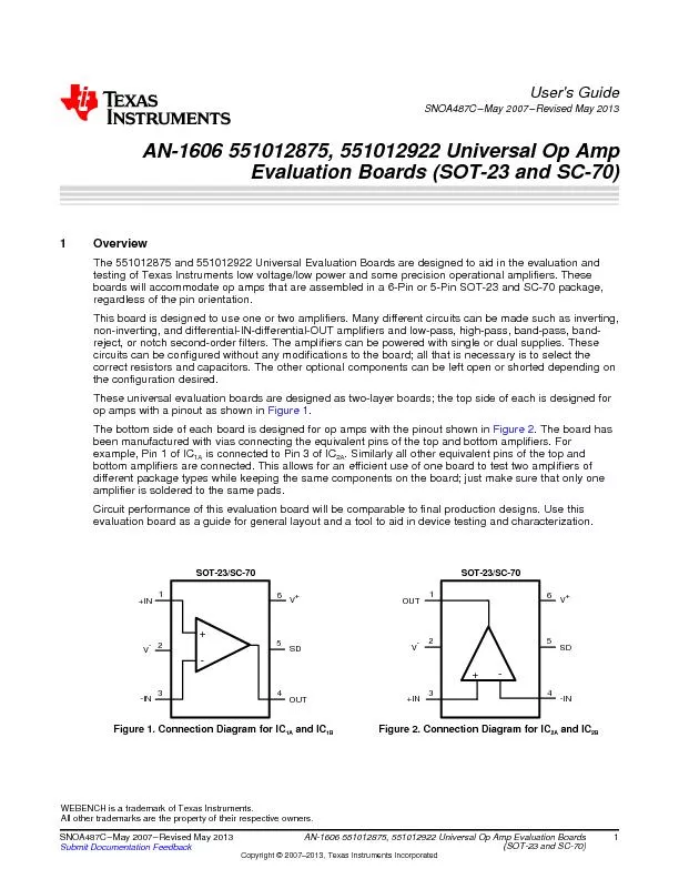
 1Overview The551012875and551012922UniversalEvaluationBoardsaredesignedtoaidintheevaluationand testingofTexasInstru ID: 433397

User'sGuide AN-1606551012875 551012922UniversalOpAmp EvaluationBoards(SOT-23andSC-70) 1Overview The551012875and551012922UniversalEvaluationBoardsaredesignedtoaidintheevaluationand testingofTexasInstru

Share:

Link:

Embed:

Download Presentation from below link

Download Pdf The PPT/PDF document "SNOA487C" is the property of its rightful owner. Permission is granted to download and print the materials on this web site for personal, non-commercial use only, and to display it on your personal computer provided you do not modify the materials and that you retain all copyright notices contained in the materials. By downloading content from our website, you accept the terms of this agreement.


Presentation Transcript

User'sGuide SNOA487C–May2007–RevisedMay2013 AN-1606551012875,551012922UniversalOpAmp EvaluationBoards(SOT-23andSC-70) 1Overview The551012875and551012922UniversalEvaluationBoardsaredesignedtoaidintheevaluationand testingofTexasInstrumentslowvoltage/lowpowerandsomeprecisionoperationalamplifiers.These boardswillaccommodateopampsthatareassembledina6-Pinor5-PinSOT-23andSC-70package, regardlessofthepinorientation. Thisboardisdesignedtouseoneortwoamplifiers.Manydifferentcircuitscanbemadesuchasinverting, non-inverting,anddifferential-IN-differential-OUTamplifiersandlow-pass,high-pass,band-pass,band- reject,ornotchsecond-orderfilters.Theamplifierscanbepoweredwithsingleordualsupplies.These circuitscanbeconfiguredwithoutanymodificationstotheboard;allthatisnecessaryistoselectthe correctresistorsandcapacitors.Theotheroptionalcomponentscanbeleftopenorshorteddependingon theconfigurationdesired. Theseuniversalevaluationboardsaredesignedastwo-layerboards;thetopsideofeachisdesignedfor opampswithapinoutasshowninFigure1. ThebottomsideofeachboardisdesignedforopampswiththepinoutshowninFigure2.Theboardhas beenmanufacturedwithviasconnectingtheequivalentpinsofthetopandbottomamplifiers.For example,Pin1ofIC1AisconnectedtoPin3ofIC2A.Similarlyallotherequivalentpinsofthetopand bottomamplifiersareconnected.Thisallowsforanefficientuseofoneboardtotesttwoamplifiersof differentpackagetypeswhilekeepingthesamecomponentsontheboard;justmakesurethatonlyone amplifierissolderedtothesamepads. Circuitperformanceofthisevaluationboardwillbecomparabletofinalproductiondesigns.Usethis evaluationboardasaguideforgenerallayoutandatooltoaidindevicetestingandcharacterization. SOT-23/SC-70 SOT-23/SC-70 Figure1.ConnectionDiagramforIC1AandIC1B Figure2.ConnectionDiagramforIC2AandIC2B WEBENCHisatrademarkofTexasInstruments. Allothertrademarksarethepropertyoftheirrespectiveowners. 1 SNOA487C–May2007–RevisedMay2013 AN-1606551012875,551012922UniversalOpAmpEvaluationBoards (SOT-23andSC-70) SubmitDocumentationFeedback Copyright©2007–2013,TexasInstrumentsIncorporated HardwareSetupwww.ti.com 2HardwareSetup 2.1ComponentNotation ThepinsofthefootprintforIC1AareconnectedtotheequivalentpinsforthefootprintofIC2Aandthesame istrueforIC1BandIC2BTherefore,thisapplicationreportwillrefertotheamplifierinIC1AorIC2AasAmpA andtheamplifierinIC1BorIC2BasAmpB.ThesubscriptofthePCBcomponentreferstothespecific amplifier;forexample,R4AisusedforAmpAandR4BforAmpB.Inthisdocument,componentswillbe referredto,asanexample,C3.IfusingAmpAthisreferstocomponentC3A,ifusingAmpBthisrefersto componentC3B. Insomecircuits,aresistorwillbeinstalledwherethePCBislabeledforacapacitororacapacitorwillbe installedwherearesistorislabeled.Forexample,CR6indicatesthatacapacitorshouldbeintheR6 position.RC5meansthataresistorwillbeinstalledintheC5position. 2.2Power PowerisappliedtothepointslabeledVí,GND,andV+.Ifasinglesupplyisused,thenVíshouldbe connectedtoGND.Avirtualground,halfwaybetweenthepositivesupplyvoltageandground,isthe referencepointfortheinputandoutputvoltages.Theoutputvoltageswingsaboveandbelowthisvirtual ground.Single-supplyoperationrequiresthegenerationofthisvirtualground,usuallyatavoltageequalto V+/2.ThecircuitinFigure3canbeusedtogenerateV+/2;R1andR2shouldbeofequalvalues.This junctionalongwithcapacitorC1willformalow-passfilterusedtoeliminateconductednoiseortransients onthepositivesupplyrail. Figure3.SingleSupplyVirtualGround 2.3OpAmp SolderanopamptoeithertheIC1AorIC2Aposition.Ifbuildingacircuitrequiringtwoopamps,solderan additionalopamptoeitherIC1BorIC2B.ThecorrespondingpinoutisshownoneachsideofthePCB. 2.4Bypassing Installthefollowingcapacitors: C6A,C9A,C6B,C9B:0.1µF C7A,C8A,C7B,C8B:1µF 2.5Shutdown TousetheshutdownfeatureoftheamplifierineithertheSOT-23ortheSC-70package,installaresistor atR15andanoptionalcapacitoratC11.TheshutdownvoltageisappliedatS/D-AorS/D-Bdependingon thepackageoftheamplifierbeingused. 2 AN-1606551012875,551012922UniversalOpAmpEvaluationBoards SNOA487C–May2007–RevisedMay2013 (SOT-23andSC-70) SubmitDocumentationFeedback Copyright©2007–2013,TexasInstrumentsIncorporated www.ti.comCircuitConfigurations 2.6InputandOutput SMAconnectorsareusedfortheinputandoutputofsignals.TheyarelocatedontheedgesofthePCB. 3CircuitConfigurations 3.1Non-InvertingAmplifier C3 Short R4 Short R5 Short R8 InputTermination R7 Outputseriesresistance(usedformatchingtransmissionlinesorisolation) R14 GainResistor R12 GainResistor Figure4.Non-InvertingAmplifier Where: (1) 3 SNOA487C–May2007–RevisedMay2013 AN-1606551012875,551012922UniversalOpAmpEvaluationBoards (SOT-23andSC-70) SubmitDocumentationFeedback Copyright©2007–2013,TexasInstrumentsIncorporated CircuitConfigurationswww.ti.com 3.2InvertingAmplifier C3 Short R9 Short R13 Short R8 InputTermination R7 Outputseriesresistance(usedformatchingtransmissionlinesorisolation) R14 GainResistor R11 GainResistor Figure5.InvertingAmplifier Where: (2) 3.3RegisterCalculations InputImpedance:SetRTtothedesiredinputimpedance.CalculateR8where: (3) TocanceltheinputbiascurrentsetR6tothevaluecalculatedwiththefollowingformula: (4) 3.4ActiveFilterApplications BothSallen-KeyandMultipleFeedbackfilterscanbebuiltonthisPCB.Todesignafilter,usethe WEBENCH™toolatwww.ti.com.Performanceathighfrequenciesislimitedtothegainbandwidthproduct oftheamplifier,butwithinthisfrequencyrange,theseactivefilterscanachieveverygoodaccuracy,iflow- toleranceresistorsandcapacitorareused. 4 AN-1606551012875,551012922UniversalOpAmpEvaluationBoards SNOA487C–May2007–RevisedMay2013 (SOT-23andSC-70) SubmitDocumentationFeedback Copyright©2007–2013,TexasInstrumentsIncorporated www.ti.comCircuitConfigurations 3.5Sallen-KeyLow-PassFilter C3 Short R13 Short R7 Outputseriesresistance(usedformatchingtransmissionlinesorisolation) R8 InputTermination SetthefollowingasdeterminedusingWEBENCH:R4,R5,CR6,R14,R12 Figure6.Sallen-KeyLow-PassFilter 3.6MultipleFeedbackLow-PassFilter Note:Ifneeded,aninputterminationresistorwillneedtobesolderedontotheSMAconnectorbetween thesignalpinandthegroundpin. R6 Short R13 Short R9 Short C5 Short R7 Outputseriesresistance(usedformatchingtransmissionlinesorisolation) SetthefollowingasdeterminedusingWEBENCH:RC3,CR8,R4,R11,C10 Figure7.MultipleFeedbackLow-PassFilter 5 SNOA487C–May2007–RevisedMay2013 AN-1606551012875,551012922UniversalOpAmpEvaluationBoards (SOT-23andSC-70) SubmitDocumentationFeedback Copyright©2007–2013,TexasInstrumentsIncorporated CircuitConfigurationswww.ti.com 3.7Sallen-KeyHigh-PassFilter C3 Short R13 Short R14 Short R7 Outputseriesresistance(usedformatchingtransmissionlinesorisolation) R8 InputTermination SetasdeterminedusingWEBENCH:CR4,CR5,RC5,R6 Figure8.Sallen-KeyHigh-PassFilter 3.8MultipleFeedbackHigh-PassFilter Note:Ifneeded,aninputterminationresistorwillneedtobesolderedontotheSMAconnectorbetween thesignalpinandthegroundpin. R9 Short R4 Short R7 Outputseriesresistance(usedformatchingtransmissionlinesorisolation) SetthefollowingasdeterminedusingWEBENCH:C3,R8,C5,CR11,R14 Figure9.MultipleFeedbackHigh-PassFilter 6 AN-1606551012875,551012922UniversalOpAmpEvaluationBoards SNOA487C–May2007–RevisedMay2013 (SOT-23andSC-70) SubmitDocumentationFeedback Copyright©2007–2013,TexasInstrumentsIncorporated www.ti.comCircuitConfigurations 3.9Sallen-KeyBand-PassFilter C3 Short R13 Short R7 Outputseriesresistance(usedformatchingtransmissionlinesorisolation) R8 InputTermination SetasdeterminedusingWEBENCH:R4,C4,CR5,R6,RC5,R14,R12 Figure10.Sallen-KeyBand-PassFilter 3.10MultipleFeedbackBand-PassFilter Note:Ifneeded,aninputterminationresistorwillneedtobesolderedontotheSMAconnectorbetween thesignalpinandthegroundpin. R6 Short R13 Short R9 Short R4 Short R7 Outputseriesresistance(usedformatchingtransmissionlinesorisolation) SetthefollowingasdeterminedusingWEBENCH:RC3,R8,C5,CR11,R14 Figure11.MultipleFeedbackBand-PassFilter 7 SNOA487C–May2007–RevisedMay2013 AN-1606551012875,551012922UniversalOpAmpEvaluationBoards (SOT-23andSC-70) SubmitDocumentationFeedback Copyright©2007–2013,TexasInstrumentsIncorporated ApplicationsUsingTwoAmplifierswww.ti.com 4ApplicationsUsingTwoAmplifiers 4.1Two-AmplifierFilters FiltersusingtwoamplifierscanbebuiltbyconnectingtheoutputofAmpAtotheinputofAmpB. 4.2Single-EndedtoDifferentialConversion ThecircuitinFigure12willconvertasingle-endedsignaltoadifferentialsignal.Thisisdonebyusingthe combinationofaninvertingamplifierandanon-invertingamplifier.Eachamplifiergeneratesoutputsignals ofequalmagnitudebutofoppositepolarity.Thistopologyisusefulinapplicationswherethesignalsource issingle-ended,buttheADCrequiresadifferentialinput.Theboardwillneedtobemodifiedby connectingInputAtoInputBwithajumperwire. Figure12.Single-EndedtoDifferentialConversion 8 AN-1606551012875,551012922UniversalOpAmpEvaluationBoards SNOA487C–May2007–RevisedMay2013 (SOT-23andSC-70) SubmitDocumentationFeedback Copyright©2007–2013,TexasInstrumentsIncorporated www.ti.comApplicationsUsingTwoAmplifiers 4.3DifferentialInput,DifferentialOutput,Non-Inverting Combiningtwonon-invertingamplifierswithacommonfeedbacknetwork,asshowninFigure13,formsa non-invertingamplifierwithadifferentialinputandadifferentialoutput.Throughtheinherentcancellation ofthetwoopampcommon-modeerrorsignalsthisconfigurationfullyexploitsthenoisereductionbenefits ofCMRR.Inadditiontheoutputvoltageswingisdoubledanddependingontheopampused,the bandwidthandslewratemayalsobeincreased,whilemaintainingtheoriginalgainbandwidth specification. Figure13.DifferentialInput,DifferentialOutput,Non-Inverting 9 SNOA487C–May2007–RevisedMay2013 AN-1606551012875,551012922UniversalOpAmpEvaluationBoards (SOT-23andSC-70) SubmitDocumentationFeedback Copyright©2007–2013,TexasInstrumentsIncorporated 551012875-001Schematicwww.ti.com 5551012875-001Schematic Figure14.551012875-001Schematic 10 AN-1606551012875,551012922UniversalOpAmpEvaluationBoards SNOA487C–May2007–RevisedMay2013 (SOT-23andSC-70) SubmitDocumentationFeedback Copyright©2007–2013,TexasInstrumentsIncorporated

Related Contents


Next Show more