PDF-Bidirectional, ZeroDrift,
Current Sense Amplifier
Data Sheet
AD8418
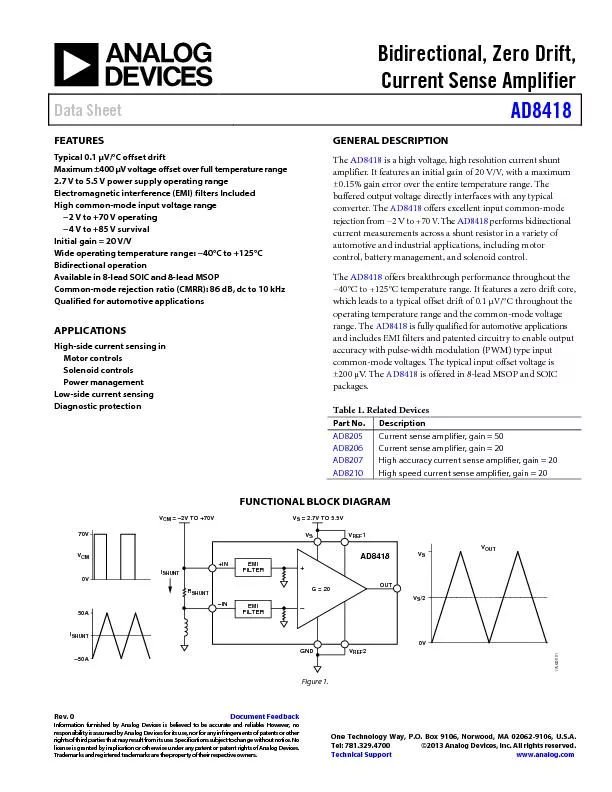
FEATURESTypical 01
Download Presentation
"Bidirectional, ZeroDrift," is the property of its rightful owner. Permission is granted to download and print materials on this website for personal, non-commercial use only, provided you retain all copyright notices. By downloading content from our website, you accept the terms of this agreement.
Presentation Transcript
Transcript not available.