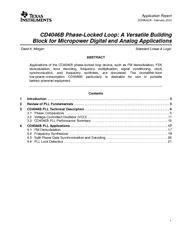
/
Applications of the CD4046B phase-locked loop device, such as FM demod Applications of the CD4046B phase-locked loop device, such as FM demod

Applications of the CD4046B phase-locked loop device, such as FM demod - PDF document

danika-pritchard
danika-pritchard . @danika-pritchard
Follow
523 views
Uploaded On 2015-08-27

Applications of the CD4046B phase-locked loop device, such as FM demod - PPT Presentation

1Introduction 2Review of PLL Fundamentals33CD4046B PLL Technical Description431Phase Comparators532VoltageControlled Oscillator VCO1133CD4046B PLL Performance Summary124CD4046B ID: 116730

1Introduction

Share:

Link:

Embed:

Download Presentation from below link

Download Pdf The PPT/PDF document "Applications of the CD4046B phase-locked..." is the property of its rightful owner. Permission is granted to download and print the materials on this web site for personal, non-commercial use only, and to display it on your personal computer provided you do not modify the materials and that you retain all copyright notices contained in the materials. By downloading content from our website, you accept the terms of this agreement.


Presentation Transcript

Applications of the CD4046B phase-locked loop device, such as FM demodulation, FSKdemodulation, tone decoding, frequency multiplication, signal conditioning, clocksynchronization, and frequency synthesis, are discussed. The monolithic-formlow-power-consumption CD4046B particularly is desirable for use in portablebattery-powered equipment. 1Introduction . . . . . . . . . 2Review of PLL Fundamentals33CD4046B PLL Technical Description43.1Phase Comparators53.2Voltage-Controlled Oscillator (VCO)113.3CD4046B PLL Performance Summary124CD4046B PLL Applications174.1FM Demodulation4.2Frequency Synthesizer194.3Split-Phase Data Synchronization and Decoding204.4PLL Lock Detection21 SCHA002A CD4046B Phase-Locked Loop: A Versatile Building Block for Micropower Digital and Analog ApplicationsList of Figures1PLL Block Diagram . . . . . . 2CD4046B PLL Block Diagram43CD4046B PLL Phase Comparator Section Schematic54Phase Comparator I Characteristics at LPF Output65Typical Waveforms for CD4046B PLL Employing Phase Comparator I 6Typical Waveforms for CD4046B PLL Employing Phase Caparator II . . . 7Phase Comparator II State Diagram98CD4046B VCO Section Schematic119Component-Selection Criteria1610FM Demodulator . . . . . . 11FM Demodulator Voltage Waveforms1812Low-Frequency Synthesizer with Three-Decade Programmable Divider1913Frequency-Synthesizer Waveforms2014Split-Phase Data Synchronization and Decoding2115Lock-Detection Circuit . 16Lock-Detection-Circuit Waveforms23List of Tables1Maximum Ratings and General Operating Characteristics132 VCO Electrical Characteristics133 Comparator Electrical Characteristics144Phase Comparator Comparison15 SCHA002A CD4046B Phase-Locked Loop: A Versatile Building Block for Micropower Digital and Analog Applications1Introduction2Review of PLL Fundamentalscomparator, low-pass filter (LPF), and voltage-controlled oscillator (VCO). All parts areconnected to form a closed-loop frequency-feedback system. Ve(t)VCO ControlVoltage Figure 1.PLL Block Diagramoperate at a set frequency, f, called the center frequency. When an input signal is applied to thefrequency and generates an error voltage proportional to the phase and frequency difference ofthe input signal and the VCO. The error voltage, Ve(t), is filtered and applied to the control inputof the VCO. Vd(t) varies in a direction that reduces the frequency difference between the VCOand signal-input frequency. When the input frequency is sufficiently close to the VCO frequency,phase difference. The range of frequencies over which the PLL can maintain this locked SCHA002A CD4046B Phase-Locked Loop: A Versatile Building Block for Micropower Digital and Analog Applications3CD4046B PLL Technical DescriptionFigure 2 shows a block diagram of the CD4046B, which has been implemented on a singlemonolithic integrated circuit. The PLL structure consists of a low-power, linear VCO and twodifferent phase comparators, having a common signal-input amplifier and a common comparatorinput. A 5.2-V Zener diode is provided for supply regulation, if necessary. The VCO can beF suffixes), 16-lead dual-in-line plastic packages (E suffix), 16-lead small outline package (NSRsuffix) and in chip form (H suffix). Comparator InSignal InV (see Figure 10) SourceFollower NCD4046BR3C2R1R2Inhibit 234567891013141516 Figure 2.CD4046B Block Diagram SCHA002A CD4046B Phase-Locked Loop: A Versatile Building Block for Micropower Digital and Analog Applications3.1Phase ComparatorsMost PLL systems utilize a balanced mixer, composed of well-controlled analog amplifiers for[logic 0 30% (V 70% (V Comparator II Out Phase Comparator IIPhase Comparator IComparator InputInput – Amplifier Q Q SignalInput Phase Comparator I OutV RRS RSRRS SR pn Figure 3.CD4046B Phase-Comparator Section Schematic SCHA002A CD4046B Phase-Locked Loop: A Versatile Building Block for Micropower Digital and Analog Applicationsbalanced mixer. To maximize the lock range, the signal- and comparator-input frequencies mustare close to harmonics of the VCO center frequency. A second characteristic is that the phaseand is 90 degrees at the center frequency. Figure 4 shows the typical, triangular,phase-to-output response characteristic of phase comparator I. Typical waveforms for a Inputs Phase DifferenceAverage Output Voltage90180Figure 4.Phase Comparator I Characteristics at LPF Output SCHA002A CD4046B Phase-Locked Loop: A Versatile Building Block for Micropower Digital and Analog Applications Signal Input (Terminal 14)VCO Output (Terminal 4) = Comparator Input (Terminal 3)Phase Comparator I Output (Terminal 2)VCO Input (Terminal 9) =Figure 5.Typical Waveforms for the CD4046B Employing Phase Comparator I or down to V, respectively. This type of phase comparator acts only on the positive edgescomparator. If the signal-input frequency is higher than the comparator-input frequency, thep-MOS output driver is maintained on continuously. If the signal-input frequency is lower thanthe comparator-input frequency, the n-MOS output driver is maintained on continuously. If thedifference. If the signal- and comparator-input frequencies are the same, but the signal inputcorresponding to the phase difference. Subsequently, the capacitor voltage of the LPFequal in both phase and frequency. At this stable operating point, both p-MOS and n-MOSoutput drivers remain off, and the phase-comparator output becomes an open circuit and holdsthe voltage on the capacitor of the LPF constant. Moreover, the signal at the phase-pulsescomparator II, no phase difference exists between signal and comparator input over the full VCOfrequency range. Moreover, the power dissipation due to the LPF is reduced when this type ofphase comparator is used because both the p-MOS and n-MOS output drivers are off for mostto the capture range, independent of the LPF. With no signal present at the signal input, the SCHA002A CD4046B Phase-Locked Loop: A Versatile Building Block for Micropower Digital and Analog ApplicationsPhase Comparator II Output(Terminal 13) Phase Pulse (Terminal 1)92CS-20011R1 NOTE A:Dashed line is an open-circuit condition.Signal Input (Terminal 14)VCO Output (Terminal 4) = Comparator Input (Terminal 3)VCO Input (Terminal 9) = Figure 6.Typical Waveforms for the CD4046Bcomparator. The number at the top inside each circle represents the state of the comparator,the left and right numbers, respectively, at the bottom of each circle. The transitions from onedown, respectively. The state diagram assumes that only one transition on either the signal inputor the comparator input occurs at any instant. States 3, 5, 9, and 11 represent the condition atn devices are off and the phase-pulses output (terminal 1) is high. The condition at thephase-pulses output for all other states is low. SCHA002A CD4046B Phase-Locked Loop: A Versatile Building Block for Micropower Digital and Analog Applications   1004002013105001210900CCCCCCCCCCCCIIIIIIIIIII Unit On in States 2, 4, 10, 12 Unit On in States 3, 5, 9, 11Phase-Pulses Output (Pin 1) High in States 1, 6, 7, 8 and Low in States 2, 3, 4, 5, 9, 10, 11, 121 Transition on Signal Input1 Transition on Comparator Input 10I Logic State ofSignal Input (Pin 14) State Number  810  01 Logic State ofComparator Input (Pin 3) Figure 7.Phase Comparator II State Diagram SCHA002A CD4046B Phase-Locked Loop: A Versatile Building Block for Micropower Digital and Analog Applicationsdifference. Section III depicts the condition when the comparator input leads the signal input inand comparator-input signals are of the same frequency, but differ slightly in phase.its high-impedance output condition (state 1), as shown in Figures 7 and 6, respectively. Thesection I, the p-device stays on for a time corresponding to the phase difference between thecomparator input goes high first, while the signal input is low, bringing the comparator to state 2.n-device being on for a time corresponding to the phase difference between the signal and SCHA002A CD4046B Phase-Locked Loop: A Versatile Building Block for Micropower Digital and Analog Applications3.2Voltage-Controlled Oscillator (VCO)Figure 8 shows the schematic diagram of the VCO. To ensure low system-power dissipation, it isdesirable that the LPF consume little power. For example in an RC filter, this requirementdictates that a high-value R and a low-value C be used. However, the VCO input must not loaddown or modify the characteristics of the LPF. Because the VCO design shown in Figure 8 was DemodulatedOutputVCO InInhibitVp2p1Inh Gate 1Gate 2 Inh 123459104675 Figure 8.CD4046B VCO Section Schematic SCHA002A CD4046B Phase-Locked Loop: A Versatile Building Block for Micropower Digital and Analog ApplicationsThe VCO circuit shown in Figure 8 operates as follows; when the inhibit input is low, p3 is turnedfull on, effectively connecting the sources of p1 and p2 to Vnetwork. External resistor R2 adds an additional constant current through p1; this current offsetscurrent of p2 is effectively equal to the current through p1, independent of the drain voltage atof the capacitor goes negative and discharges rapidly through the drain diode of the off n device.Subsequently, a new half cycle starts. Because inverters 1 and 5 have the same transfer points,In order not to load the LPF, a source-follower output of the VCO input voltage is providedthe inhibit input enables the VCO and the source follower, while a logic 1 turns off the VCO and3.3CD4046B Performance Summarycharacteristics, are shown in Table 1. The VCO and comparator characteristics are shown inTables 2 and 3, respectively. Table 4 summarizes some useful formulas as a guide forusing Table 4, note that frequencies are in kilohertz, resistance is in kilohms, and capacitance is10kR1,R2,RS100pFatV50pFatV10V SCHA002A CD4046B Phase-Locked Loop: A Versatile Building Block for Micropower Digital and Analog ApplicationsTable 1.Maximum Ratings and General Operating CharacteristicsMaximum Ratings, Absolute-Maximum ValuesOperating temperature range:Ceramic package types Plastic package types Device dissipation (per package) 200 mWAll inputs . . . . . . . . ) 5 V to 15 VRecommended input voltage swing VGeneral Characteristics (Typical Values at V) 5 V to 15 VOperating supply current:Inhibit = 0: f = 5 V 70 = 10 V 600 Inhibit = 1 25 Table 2.VCO Electrical Characteristics TYPICAL VALUES AT = 25 Maximum frequency 1.2 MHz Temperature stability 600 ppm/ C 2.5 V) 1% Center frequency Programmable with R1 and C1 Frequency range Programmable with R1, R2, and C2 Input resistance 10 Output voltage 10 Vp-p Duty cycle 50% Rise and fall times 50 ns Out p utcurrentca p ability Logic 1: Drive at VO 9.5 V –1.8 mA Output current capability Logic 0: Sink at VO 0.5 V 2.6 mA Offset voltage (V 1.5 V SCHA002A CD4046B Phase-Locked Loop: A Versatile Building Block for Micropower Digital and Analog ApplicationsTable 3.Comparator Electrical CharacteristicsCOMPARATOR CHARACTERISTICS TYPICAL VALUES AT = 25 Signal Input Input impedance 400 k Input sensitivity AC coupled 400 mV DCcou p led Logic 0: 30% (VDD– DC coupled Logic 1: 70% (VDD– Com p aratorin p utlevels(terminal3) Logic 0: 30% (VDD– Comparator - input levels (terminal 3) Logic 1: 70% (VDD– Output Current Capability Comparator I (terminal 2) and comparator II (terminal 13) = 9.5 V –1.8 mA = 0.5 V 2.6 mA Comparator II phase pulses (terminal 1) = 9.5 V –1.8 mA = 0.5 V 1.4 mA SCHA002A CD4046B Phase-Locked Loop: A Versatile Building Block for Micropower Digital and Analog ApplicationsTable 4.Phase Comparator Comparison USING PHASE COMPARATOR I USING PHASE COMPARATOR II CHARACTERISTICS VCOWITHOUT OFFSETR2 = VCO WITH OFFSET VCOWITHOUT OFFSETR2 = VCO WITH OFFSET VCO frequency fofV VCO Input Voltage fV VCO Input Voltage fofV VCO Input Voltage fV o2fL VCO Input Voltage For no signal input to center frequency, f lowest operating frequency, f Frequency-lock range, 2fL = full VCO frequency range Frequency capture range, 2fC R3 1 = R3 C2C2 In 11 2fL1  See Notes 1 and 2 Loop filter-component selection R3OutR4 C2 For 2fC, see Note 2 fC = fL Phase angle between signaland comparator inputs 90 degrees at center frequency (fo), approximating0 degree and 180 degrees at ends of lock range(2fL) Always 0 degrees in lock Locks on harmonics of center frequency Yes Signal input noise rejection High Low VCO component selection Given: f with Figure 9a Given: f and f Calculate fCalculatemin min fofLfO–fL min Given: f Calculate f from the with Figure 9a Given: f and fCalculatemin min NOTES:1.F. Gardner, Phase-Lock Techniques, John Wiley and Sons, New York, 1966.2.G.S. Moschytz, Miniaturized RC Filters Using PLL, May 1965. SCHA002A CD4046B Phase-Locked Loop: A Versatile Building Block for Micropower Digital and Analog ApplicationsIn addition to the design information in Tables 1, 2, and 3, refer to Figure 9 for R1, R2, and C1component selections. The use of Table 4 in designing a PLL system using the CD4046B for (c) Typical f vs R2/R1 (b) Typical Frequency Offset vs C1 (a) Typical Center Frequency vs C1 Figure 9.Component-Selection Criteria SCHA002A CD4046B Phase-Locked Loop: A Versatile Building Block for Micropower Digital and Analog Applications4CD4046B PLL Applicationsas FM demodulators, frequency synthesizers, split-phase data synchronization and decoding,4.1FM Demodulationsignal. The VCO input voltage, which is the filtered error voltage from the phase detector,FM demodulator. For this example, an FM signal consisting of a 10-kHz carrier frequency wasmodulated by a 400-Hz audio signal. The total FM signal amplitude is 500 mV, therefore, the Low-Pass Filter346 1178 Comparator I Total Current Drain: = 132 Figure 10.FM Demodulator SCHA002A CD4046B Phase-Locked Loop: A Versatile Building Block for Micropower Digital and Analog ApplicationsThe formulas in Table 4 for phase comparator I with R2 = frequency, 10 kHz. The 500-pF value of capacitor C1 was found by assuming R1 = 100 k = 5 V. 23C2 0.4kHzF) determine this capture frequency.Figure 11 shows the performance of the FM-demodulator circuit of Figure 10 at a 4-dB S/N ratio.The demodulated output is taken off the VCO-input source follower using resistor RS = 100 k 400-Hz Audio TransmittedFigure 11.FM Demodulator Voltage Waveforms SCHA002A CD4046B Phase-Locked Loop: A Versatile Building Block for Micropower Digital and Analog Applications4.2Frequency Synthesizersystem is in lock, the signal and comparator inputs are at the same frequency, and f = N CD4046B 1 kHZ117 Tens 1297321297321297321010 RD S 003 Outputf = N 1 kHzDivide-by-NLow-Pass FilterR3100 k5 kR110 k1 Figure 12.Low-Frequency Synthesizer With Three-Decade Programmable Divider SCHA002A CD4046B Phase-Locked Loop: A Versatile Building Block for Micropower Digital and Analog ApplicationsTherefore, the frequency range of this synthesizer is 3 kHz to 999 kHz in 1-kHz increments,which is programmable by the switch position of the divide-by-n counter.Using the formulas for phase comparator II shown in Table 4, the VCO is set up to cover a rangelocking for step changes in frequency. Figure 13 shows the waveforms during switching betweenswitch-position hundreds in the divide by-n counter. 50 ms/DIVVoltage Figure 13.Frequency-Synthesizer Waveforms4.3Split-Phase Data Synchronization and DecodingFigure 14 shows another application of the CD4046B for split-phase data synchronization andduration of each bit and, therefore, the periodic bit rate, essentially is constant. To detect andcan be utilized to recover the clock and the data. Timing information is contained in the datameaning for timing recovery. The phase of the signal determines the binary bit weight. A binary 0or 1 is a positive or negative transition, respectively, during a bit interval in split-phase data SCHA002A CD4046B Phase-Locked Loop: A Versatile Building Block for Micropower Digital and Analog Applications Q BCDE Split-PhaseDataR1VCOPhaseComparatorIIR3 DVCO OutDiffR2C1FF1Low-Pass Filter Q CLDFF2CLC1 DataOutClock Out FF3CLD Figure 14.Split-Phase Data Synchronization and DecodingAs shown in Figure 14, the split-phase data input, A, is first differentiated to mark the locations ofthe data transitions. The differentiated signal, B, which is twice the bit rate, is gated into thedivides the VCO frequency by two. During the on intervals, the PLL tracks the differentiatedsignal B. During the off intervals, the PLL remembers the last frequency present and still4.4PLL Lock Detectionunlocked condition, respectively. This signal could, in turn, activate circuitry using a locked PLL SCHA002A CD4046B Phase-Locked Loop: A Versatile Building Block for Micropower Digital and Analog ApplicationsFigure 15 shows a lock-detection scheme for the CD4046B. The signal input is switchedTherefore, the PLL locks and unlocks on the 10-kHz and 20-kHz signals, respectively. When thePLL is in lock, the output of phase comparator I is low, except for some very short pulses thatresult from the inherent phase difference between the signal and comparator inputs; thesame phase difference. This low condition of phase comparator I is detected by the 2SignalIn Comparator IICD4001ACD4001ACD4001ACD4001A 14CD4046BPhaseComparator I Figure 15.Lock-Detection Circuit SCHA002A CD4046B Phase-Locked Loop: A Versatile Building Block for Micropower Digital and Analog Applications Signal Input 20Control Voltage Governing Vertical: 5 V/DivFigure 16.Lock-Detection-Circuit Waveforms IMPORTANT NOTICETexas Instruments Incorporated and its subsidiaries (TI) reserve the right to make corrections, modifications,enhancements, improvements, and other changes to its products and services at any time and to discontinueorders and should verify that such information is current and complete. All products are sold subject to TI’s termsTI warrants performance of its hardware products to the specifications applicable at the time of sale inaccordance with TI’s standard warranty. Testing and other quality control techniques are used to the extent TIdeems necessary to support this warranty. Except where mandated by government requirements, testing of allTI assumes no liability for applications assistance or customer product design. Customers are responsible fortheir products and applications using TI components. To minimize the risks associated with customer productsand applications, customers should provide adequate design and operating safeguards.TI does not warrant or represent that any license, either express or implied, is granted under any TI patent right,copyright, mask work right, or other TI intellectual property right relating to any combination, machine, or processin which TI products or services are used. Information published by TI regarding third–party products or servicesdoes not constitute a license from TI to use such products or services or a warranty or endorsement thereof.Use of such information may require a license from a third party under the patents or other intellectual propertyof the third party, or a license from TI under the patents or other intellectual property of TI.Reproduction of information in TI data books or data sheets is permissible only if reproduction is withoutalteration and is accompanied by all associated warranties, conditions, limitations, and notices. Reproductionof this information with alteration is an unfair and deceptive business practice. TI is not responsible or liable forsuch altered documentation.Resale of TI products or services with statements different from or beyond the parameters stated by TI for thatproduct or service voids all express and any implied warranties for the associated TI product or service andTexas InstrumentsPost Office Box 655303Dallas, Texas 75265 2003, Texas Instruments Incorporated