/
may be cascaded to minimize intercon-nects to the microcontroller, hen may be cascaded to minimize intercon-nects to the microcontroller, hen

may be cascaded to minimize intercon-nects to the microcontroller, hen - PDF document

danika-pritchard
danika-pritchard . @danika-pritchard
Follow
392 views
Uploaded On 2015-08-16

may be cascaded to minimize intercon-nects to the microcontroller, hen - PPT Presentation

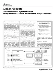
For the power drive TI offers theTPIC2601 a 6channel commonsourcepower DMOS array with gate protectionCoupled with the TPIC46L0102 it provides power and protection capabilitiesfor switching me ID: 108427

For the power drive

Share:

Link:

Embed:

Download Presentation from below link

Download Pdf The PPT/PDF document "may be cascaded to minimize intercon-nec..." is the property of its rightful owner. Permission is granted to download and print the materials on this web site for personal, non-commercial use only, and to display it on your personal computer provided you do not modify the materials and that you retain all copyright notices contained in the materials. By downloading content from our website, you accept the terms of this agreement.


Presentation Transcript

may be cascaded to minimize intercon-nects to the microcontroller, hence reduc-ing costs. When using this configuration,serial data is input to the device and istransferred out the serial data output For the power drive, TI offers theTPIC2601, a 6-channel common-sourcepower DMOS array with gate protection.Coupled with the TPIC46L01/02, it pro-vides power and protection capabilitiesfor switching medium-current loads. TheTPIC46L01/02 and TPIC2601 combina-tion provides effective switching of thefuel injectors by means of a parallel loadinterface, fault detection and protection,and an efficient power output stage. Faultisolation features included in theTPIC46L01/02 are shorted and open-load detection, and over and under-bat-tery voltage shutdown; all are real-timefault indicators via a fault interrupt to themicrocontroller. Load fault protection isprovided by disabling the gate output forthe TPIC46L01 or transitioning to a lowduty cycle pulse-width-modulatedTo enable parallel data transfer, data istransferred directly from the parallelinterface inputs (IN0±IN5) to each re-spective gate output asynchronously. Thechannel is turned ON with a logic highand OFF with a logic low. The parallelinput port and serial control data areOR'ed in the output control register toallow either interface to control the gaterequired for parallel control, it is stillavailable to transfer fault data back to themicrocontroller. Figure 2. Circuit Schematic of the TPIC46L02 Pre-FET Driver and the TPIC2601 Power+ Array 10 mF 10 mF mF 10 kW FLT VVCOMPIN1IN2IN3IN4IN5CS BATGATE0GATE1GATE2GATE3GATE4GATE5Injector On/OffPre-FET DRIVERSingle Point GNDBAT Returnseries resistance whenBAT 272625242322212019181716151234571091312151447 W12 W ECU Normal Operation of a Fuel InjectorMicrocontroller inputs are provided tothe predriver via the parallel input termi-nals as shown in Figure 2. To turn an out-put on, the appropriate parallel input istransitioned from low to high. Trace 1 ofFigure 3 shows an example waveform forthe IN0 input. Trace 2 shows the corre-sponding gate drive output GATE0. Thewaveform in trace 3 illustrates that thepower transistor drain current(DRAIN0), i.e. injector current, rises at arate determined by the injector induc-tance and the battery voltage. It continuesto rise until the maximum value isreached, a result of the injector resistance.Once the injector is turned off, the mag-netic field collapses inducing a voltage atDRAIN0 node of the power transistor.This voltage (trace 4) then rises until it isclamped at approximately 55 V. Figure 3. Drain Voltage and Current Figure 4. Open/Short-Fault ConditionsNote that FLT0 occurs in the second byte of data when it occurs and is available on theSDO port whenever CS transitions low toenable the serial interface. As can be seenin Figure 5, the FLT goes low when thefault occurs and then remains low. Whenthe fault occurs, the gate output turns offafter 60 s and remains off until the inputis turned off and back on.The predriver monitors the drain voltagethe inductive transient. The drain inputsare used in an internal clamp, or ªsnubº,circuit to pull up the gate. This snub cir-cuit turns the output on to dissipate theenergy stored in the injector and preventthe drain voltage from exceeding themaximum V of the power transistor.Once the gate voltage has fallen, a delaybefore the gate turns off completely.Trace 2 of Figure 3 shows the gate pull-updue to the inductive transient.transferred on the first high-to-lowtransition of SCLK with the remainingdata transferred on the falling edges of thefollowing six clocks. The CS input mustbe transitioned high after the eighth clockto load control data into the output bufferFault IsolationThe TPIC46L01/02 offers fault isolationto meet emission control requirementsplaced on today's engine control systems.The real-time monitoring comes in theform of a fault interrupt line (FLT ). Afterthe FLT goes low, the microcontroller cancheck the serial diagnostic data to isolatethe channel at fault. As can be seen inFigure 4, the output controlled by IN4(trace 4) is shorted and the outputcontrolled by IN0 is open. During normaloperation, CS is held high to disable theserial interface and to allow the device tomonitor the fault status of the load. Thefault register status is locked on the condition and have the fault dataavailable at the SDO port, the CS must golow while the fault exists. The faultinterrupt (FLT ) will remain active (seeFigure 6) until cleared by CS shorted-load fault occurs, the gate driveoutput goes into a low duty cycle PWMmode and will remain there as long as theoutput is enabled and the fault conditionis present. The FLT is refreshed when CS transitions low after the fault has beenWhen using either the serial or parallelport for control, care must be taken toensure that eight bits of data are clockedinto the SDI port if CS transitions low.Less than eight bits of data may result inunknown data being transferred into theoutput control register as CS transitionshigh. To illustrate the fault status in tracedata shown, one indicating a short presentat DRAIN4 and the other indicating anopen at DRAIN0. As CS goes low, the bitrepresentations are: left to right startingwith the most significant bit to the leastsignificant bit, over-battery (MSB),under-battery, and FLT5 to FLT0 (LSB).provided including bits for over-battery-voltage, under-battery-voltage, andshorted-load or open-load faults. As CS goes low, the first bit of fault status data(over-battery) is immediately available.The second bit of fault status data isOperation of a Shorted InjectorAmong the faults monitored is that of ashorted injector. This fault is isolatedonly when the output transistor is on.Trace 4 of Figure 7 illustrates the drain ofthe output transistor controlled by IN0shorted to VBAT. IN0 (trace 1) transitionshigh as the output is commanded to turn transferred out of SDO on the fallingedges of SCLK. Figure 6. Fault Clears Figure 5. Fault is Captured The TPIC46L01 and TPIC46L02 handleshorted-load fault conditions differently.The TPIC46L01 flags the microcontrol-ler that a fault condition exists and thegate output is automatically shut off untilthe microcontroller turns it back on. Thisreduces the on-time to approximatelys, keeping the power dissipationwithin limits and preserving the outputtransistor. When the TPIC46L02 experi-ences a shorted-load condition, it transi-tions to a low duty cycle PWM state toautomatically re-check the fault condi-tion and protect the FET from over-heat-ing. An example is shown in trace 4 ofFigure 7. This mode continues until theerror has been corrected or until themicrocontroller turns the output off. stabilize. At this time, the drain voltage iscompared to the fault reference threshold.If the drain voltage is greater than thereference of 1.25 V, then an over-currentor shorted-load condition exists. The FLT (trace 3) is transitioned low to notify themicrocontroller of the error.The drain inputs for unused channelsmust be pulled high to prevent falsereporting of open load condition. Anopen load is checked by placing a 60 current source on the drains of each of theFET's. If the load impedance is high, thecurrent source will be sufficient to pullthe drain of the transistor below the1.25 V reference threshold of thedetection circuit. A deglitch time of 60 is provided to allow the drain to stabilizebefore the test is enabled. If an open-loadfault is present, then a fault flag is issuedto the microcontroller until the fault hasbeen corrected.The test for an open load is performedonly when the output transistor is off.Under normal condition, the drain ispulled high by the load (see Figure 2).Over/Under-Battery VoltageThe predriver monitors the batteryvoltage to protect the load and powertransistor from over-battery conditions.The over-battery voltage detectionthreshold is set at 34 V. The under-batteryvoltage threshold is set at 4.8 V to protectthe output transistor and load fromthermal stress. In both cases, the devicedisables all gate outputs as long as thebattery fault condition is present. Shorteduntil the battery voltage error has beencorrected to ensure erroneous faults areFault Detection Threshold ReferenceAs mentioned previously, approximatelystabilization time), the drain voltage iscompared to an internal reference of1.25 V during the on/off time to check fora shorted/open output. In Figure 2, pin 2compare enable (Vgrounded to select the internal 1.25 Vreference. The pin is pulled high to selectthe external reference voltage comparebe used at this pin to set the fault thresholdreference to a different value. 4 Figure 7. Shorted Drain Figure 8. Over/Under-Battery Fault Conditions A key design consideration when select-ing the power output stage for thisparticular application is power dissipa-tion. The total power dissipation of thetransistor array is the sum of the power inthe on-state, plus the power resultingfrom the transient as the inductor isturned off, multiplied by the number oftransistors in the array. To illustrate,values from Figure 3 waveforms and theTPIC2601 datasheet will be used. Forsimplicity, three worst case assumptionswill be made. The first is that the draincurrent decays linearly when it is turnedoff. The second is that the maximumoperating ambient temperature is 125The third and final assumption is that aequal to 5C/W. The power dissipationparameters are given as follows: = thermal resistance junction to = thermal resistance case to = thermal resistance heatsink toBAT = maximum junction = maximum ambient operating = case temperature = heat sink/temperatureor switch off-timeAfter defining the power parameters, themaximum allowed power that can be dis-sipated by the power array depends on (1)the ambient temperature at which it oper-ates and (2) the thermal resistance fromthe FET junctions to that ambient. Theresult is as follows:Solution 1:(150C)/C/W + 0.5C/W + C/W) = 2.78 W**Total power for the packageTransistorThe on and off-time power that is dissi-pated in the transistor is a function of thedrain current I (trace 3) in Figure 3,DS(on)time power is the sum of the power duringthe ramp up (0 ± 2 ms) = 2 ms and thepower at the maximum value (2 ms ±Equation 3:PDS(on)Equation 4:PSolution 4:PEquation 2:PDS(on)(during ramp up time period) Some designs may require a differentcurrent detection level to better match aparticular power transistor's on-resis-tance or meet other system requirements.Equation 1:(TSolution 2:PSolution 3:PThe off-time power is the power duringcurrent decay which can be seen inFigure 3 when observing the IN0(trace1), the DRAIN0 current Equation 6:P = f * (3 * L * I * VBATSolution 6:P From solutions 4 and 5 above, the totalIf the information in Figure 3 were not yetavailable, i.e. the TPIC46L01/02 andTPIC2601 had not already beenincorporated into the system, thecalculation could be made from the datain the above table.The power dissipated with all six FETsconducting is 6 * 0.394 W = 2.364 W.From Solution 1, it was determined thatthe total power capacity for the packageis 2.78 W; therefore, all six powertransistors can turn on simultaneouslyand operate below the maximumallowable junction temperature of 150Solution 5:PThe TPIC44L01/02 uses a 4-bit dataword for serial transfers which allows theuser to cascade two pre-drivers tocommunicate with 8-bit words. Cascad-ing of the serial ports requires a minimumserial word operation valid for anymultiple of 4 bits. This could potentiallydouble the serial throughput whilesending and receiving data with themicrocontroller. The first stage transfersits fault data through the second stage The use of a 4-bit serial word increasesdata throughput compared to 8-bit words.Due to the absence of theover/under-battery voltage bit reporting,serial data transfer of both fault data andcontrol data information is more efficientand advantageous for 4-channelswitching requirements. Figure 9. 8-Bit Serial Word Operation IN7SCLKCS (New Data)GATE7-4 (2nd Stage)GATE3-0 (1st Stage)IN6IN5IN4IN3IN2IN1IN0N/A FLT7SDOFLT6FLT5FLT4FLT3FLT2FLT1FLT0IN712345678TPIC44L01/02 and TPIC2401Effective fuel injector drive can also beaccomplished with the TPIC44L01/02and TPIC2401. As mentioned earlier, theTPIC44L01/02 are 4-channel low-sidepre-FET drivers capable of serial orparallel interface and the TPIC2401 is a4-channel common-source power DMOSarray with gate protection. There areslight differences between the 4-and6-channel chipsets.followed by control data. As with the6-channel devices, the fault data is avail-able immediately when CS transitionslow to monitor the status of the SDO port.An example of 8-bit serial word operationcan be seen in Figure 9 when observingthe timing diagrams.The MSB of fault data is available firstwith the following bit representationsfrom left to right, FLT7 to FLT0 (LSB).The 4-channel device offers real-timefault reporting by means of the FLT interrupt line. The over/under-batteryvoltage condition results in all outputsbeing turned off and the disabling of faultreporting for shorted and open-loadconditions. With the 4-channel device,fault isolation is identical to that of the6-channel device with the exception ofover- and under-battery voltage fault bitsbeing removed from the serial fault data.An additional feature on the 4-channeldevices is an active low reset line ). The RESET line clears thefault register, the control register, and the (trace 3), and the DRAIN0 voltagefor approximately 125 the drain voltage at 60 V while the currentdecays to zero. As stated previously,assuming linear decay as the worst casescenario, the power can be calculated ifcurrent and voltage waveforms of Figuretime and multiplying by the voltage, thiswill give the equivalent: fault interrupt line when transitioned low.This provides the means to disable theoutputs and clear the device by togglingThe 6-channel (TPIC46L01/02 andTPIC2601) or 4-channel (TPIC44L01/02and TPIC2401) chipset offer an enhancedapproach to switching medium-load cur-rent applications. This dual-chip solutionprovides greater flexibility for the de-signer to select a power stage that bettermatches load requirements than may beavailable when using an integrateddevice. The TPIC46L01/02 orTPIC44L01/02 offers a parallel input in-terface to perform real-time control of theexternal power output stage in addition toproviding fault detection and protectionto prolong transistor life and increasesystem reliability. SLIT112 IMPORTANT NOTICETexas Instruments (TI) reserves the right to make changes to its products or to discontinue any semiconductorproduct or service without notice, and advises its customers to obtain the latest version of relevant informationto verify, before placing orders, that the information being relied on is current and complete.TI warrants performance of its semiconductor products and related software to the specifications applicable atthe time of sale in accordance with TI's standard warranty. Testing and other quality control techniques areutilized to the extent TI deems necessary to support this warranty. Specific testing of all parameters of eachCertain applications using semiconductor products may involve potential risks of death, personal injury, orTI SEMICONDUCTOR PRODUCTS ARE NOT DESIGNED, INTENDED, AUTHORIZED, OR WARRANTEDTO BE SUITABLE FOR USE IN LIFE-SUPPORT APPLICATIONS, DEVICES OR SYSTEMS OR OTHERCRITICAL APPLICATIONS.Inclusion of TI products in such applications is understood to be fully at the risk of the customer. Use of TIproducts in such applications requires the written approval of an appropriate TI officer. Questions concerningpotential risk applications should be directed to TI through a local SC sales office.In order to minimize risks associated with the customer's applications, adequate design and operatingTI assumes no liability for applications assistance, customer product design, software performance, orinfringement of patents or services described herein. Nor does TI warrant or represent that any license, eitherexpress or implied, is granted under any patent right, copyright, mask work right, or other intellectual propertyright of TI covering or relating to any combination, machine, or process in which such semiconductor products 1998, Texas Instruments Incorporated