/
fer speed limits by orders of magnitude beyond the fer speed limits by orders of magnitude beyond the

fer speed limits by orders of magnitude beyond the - PDF document

karlyn-bohler
karlyn-bohler . @karlyn-bohler
Follow
431 views
Uploaded On 2015-08-23

fer speed limits by orders of magnitude beyond the - PPT Presentation

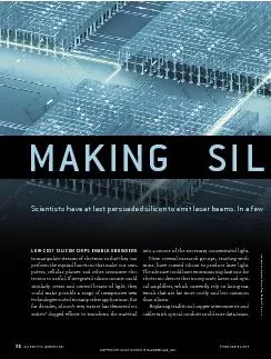
AKING capabilities of current technology For example cable modems the workhorses of household Inter net connections are currently limited to a transfer rate of about one megabyte a second Opti ID: 113682

AKING capabilities current technology.

Share:

Link:

Embed:

Download Presentation from below link

Download Pdf The PPT/PDF document "fer speed limits by orders of magnitude ..." is the property of its rightful owner. Permission is granted to download and print the materials on this web site for personal, non-commercial use only, and to display it on your personal computer provided you do not modify the materials and that you retain all copyright notices contained in the materials. By downloading content from our website, you accept the terms of this agreement.


Presentation Transcript

AKING fer speed limits by orders of magnitude beyond the capabilities of current technology. For example, cable modems, the workhorses of household Inter net connections, are currently limited to a transfer rate of about one megabyte a second. Optical de vices built on silicon chips could effortlessly trans fer oversize digital files, such as high-definition vid eos, at rates as high as 10 gigabits a second a 10,000-fold improvement. Compact sensors that include integrated circuits with silicon lasers could combine the capabilities of a diagnostic lab-on-a- chip with wireless communications to detect pol lutants, chemical warfare agents or explosives as parts of extensive environmental monitoring and security networks. In a promising military applica- LASER BEAM red and white glow in title ) was the first ever produced by a silicon device; its infrared light is invisible to the eye and is false-colored here. Silicon lasers that are integrated into microchips ( background ) could make low-cost computing with light practical. years, computers and other devices will handle light as well as electrons www.sciam.com SCIENTIFIC AMERICAN 59 BY BAHRAM JALALI COPYRIGHT 2007 SCIENTIFIC AMERICAN, INC. 60 SCIENTIFIC AMERICAN FEBRUARY 2007 tion, silicon lasers might be able to mis lead the infrared sensors of heat-seeking antiaircraft missiles to provide a cost-ef fective countermeasure against them. Laser Primer why has it tak&n so long to teach silicon this new trick? Unlike materials commonly used as host media for lasing, such as the gallium arsenide used in DVD players, silicon is not naturally or ganized to promote the two-step process that results in a coherent light beam. It cannot emit light efficiently when ener gized (the first requirement), and what ever light it does produce is incapable of amplifying light into a laser beam by “stimulating” it to create more photons. (“Laser” stands for ight mplification by timulated mission of adiation.) In a laser, an external energy source, usually light or an electric current, “pumps” the electrons in the atoms of the host medium to a higher energy level, which physicists call an upper (or excit ed) state. When these atoms return to their normal (ground) state, the extra energy is released as photons of light (el ementary quantum units of electromag netic radiation that exist simultaneously as a wave and a particle). Albert Einstein dubbed this process “spontaneous emis sion”: a phenomenon that yields pho tons that travel outward in all directions at random, giving rise to low-intensity, diffused light much like that cast by a fluorescent bulb. When one of these emitted photons passes through a group of previously pumped electrons in the host material, it triggers, or stimulates, the electrons to discharge their surplus energy all at once, a concept first pro posed in a paper published by Einstein in 1917. The resulting photons travel to gether in the same direction in synchro ny, forming a highly directional light beam. As the beam travels through oth er excited atoms in the medium, its pho tons, in turn, stimulate the emission of yet more photons in a cascade. The effect [)) Scientists have long sought a silicon chip that can handle light as deftly as it does electrons, but silicon does not produce light easily, especially concentrated laser light. Such an advance could lead to ultrafast digital data transfers, new sensor networks and many other innovations. [)) After many years of work, researchers are finally making silicon lase by using several different materials-based techniques. The birth of a novel hybrid technology silicon electrophotonics is at hand. Overview/ Silicon Lasers The lasing process is based on the quantum behavior of electrons in the outer orbitals of the atoms in a suitable material. An outer- shell electron in a single atom is energized (or “pumped”) after absorbing a photon an elementary quantum unit of light which raises it to a higher orbit and energy level ( ). An energized electron releases a photon when it drops down to a lower level. In a solid, atoms form bonds by sharing these outer electrons ( ). To achieve light amplification, the prerequisite to lasing, external energy sources pump the shared electrons to higher energy levels. As the energized electrons release photons, those photons, in turn, stimulate further photon emissions amplifying light. Photons can also be amplified when they collide with excited phonons which are quantized atomic vibrations of the crystal lattice ( ). When single atoms bond together into crystals, the character of the shared electrons’ energy levels changes to broader bands ( ) because of the effect on the electromagnetic environment of many nearby atoms. Thus, a pumped electron in a crystal jumps from one band to another. When the energies and momenta of electrons in a common lasing medium such as gallium arsenide are plotted on a graph, the energy bands line up vertically because they share the same momenta ( ). (A band describes the possible quantum states that electrons can take; each state has a quantity that can be identified with a classical momentum and that must be conserved during collisions.) The bands in silicon, in contrast, JEN CHRISTIANSEN ( this page and opposite page ); KEN EWARD BioGrafx THE CHALLENGE OF GETTING SILICON TO LASE Silicon offers enormous promise for low-cost computing with light, but its very nature makes it an unlikely lasing medium. (c8BoHFeAapdGIoFAEWDE8HAc8r8c 0DsorDaWpeoJBaGa8saWpeoJ (c8BoHFeACHFGIoFAcFs8HAc8r8 3GEJr 0H4Wo3cAdFC8c Ce8raWAaGaEJr(DW) 4e 2FsraJaAaIardLGaKaGAFIA8IFsoG8JaW8J3IardLD8IWAFI8AErLsJ8 1rFIdFIdA8JsAJodaJearJoAcorHA8AErLsJ83IardL )F8HA43eC 1WcWBFeABHJIo3cAc3ooWB 1oIW 2GG8HA43eC COPYRIGHT 2007 SCIENTIFIC AMERICAN, INC. www.sciam.com SCIENTIFIC AMERICAN 61 is analogous to the way the mass of an avalanche grows as it courses down a snow-covered mountainside. Einstein’s prediction of stimulated emission did not garner much interest until the 1950s, when physicists began to realize its potential applications in optical or photonic devices. In 1958 Charles Townes and Arthur Schawlow proposed partially surrounding a light- amplifying material with mirrors to re flect some of the photons it generated back inside. They showed that the stim ulation process then would feed on itself (as in a chain reaction). This approach, once fully developed, could create a powerful light flow with a well-defined wavelength a laser beam. Just two years later Theodore Maiman demon strated the first operational laser, made by optically pumping a ruby crystal with a powerful lamp. ilicon has proved considerably less pliant than ruby crystals or other subse quently developed lasing media. In semiconductors materials whose elec trical performance lies midway between an excellent conductor such as copper and an insulator such as rubber or cer tain ceramics electrons exist in energy bands, which are ranges of energy levels, or states, that electrons can occupy. The energy band describes the range of levels that electrons are “forbidden” or “allowed” to inhabit according to quan tum theory; the gap between permitted bands (the band gap) is a range of energy levels that the electron is forbidden to oc cupy. An electron in an atom’s outer or bital can take on energy (letting it jump to a higher band) by absorbing a photon or can release energy (dropping back down) by emitting one. Physicists clas sify these interactions as a kind of scat tering event. Imagine the energy bands as a series of buckets in which electrons sit [ see box above ]. Normally, almost all the elec trons remain in the lower energy band, or bucket, leaving the upper band nearly empty. But if a photon with energy equal to or greater than the band gap collides with an electron, it can raise the electron to the upper band. The electron hops from the lower bucket to a higher one. Light absorption, the name for this ef fect, is the basis for the way solar cells convert light into electricity. For the material to produce photons, it must receive enough energy to pump many electrons from the lower band to the upper band, causing a so-called popu lation inversion (compared with the usu al distributions present in the bands). It is unnecessary to pump the entire electron population; only the part near the top of the lower band need be affected. Engi neers often excite electrons directly by forcing electric current through a semi conductor diode. Illuminating the sub stance with an external light source, as Maiman did, can also pump electrons. have different momenta, which means that energy from an absorbed photon alone is not enough to cause an electron to jump to a higher band ( ). Instead the electron must wait until a phonon with the right extra momentum shows up to broker the transfer of energy. Unfortunately, these electrons often lose their surplus energy as heat before a suitable phonon arrives, which leads silicon to emit light inefficiently. Silicon’s low emission efficiency allows an intraband phenomenon called free carrier absorption to obstruct light amplification and lasing. When a passing photon interacts with an energized electron (a free carrier) in an upper band, one of two competing processes can occur. Either the photon can stimulate the emission of another photon, causing the electron to fall to a lower band, or the electron can simply absorb the photon, which merely moves it higher in the same band ( ), an event that does not produce another photon and thus does not promote light amplification and lasing. Gallium arsenide’s upper bands hold comparatively few electrons. When depicted on a graph, the upper band is narrow, with steeply sloped sides. Because gallium arsenide has a high emission rate (it amplifies light efficiently because its bands line up), its photon emissions easily outpace its absorptions, and thus the material amplifies light. The wider, less-steep-sided upper bands in silicon require more electrons to fill them up. Silicon, with its low emission rate (caused by its indirect lineup) and high free carrier absorption rate, is unable to amplify light. THE CHALLENGE OF GETTING SILICON TO LASE 1eeCAa3HWdDAc38GW3aA(HoBEA3HAD3aaWocA3GH8dWC8)eeGAa3HWdDAc38GW3aA(HoBEA3HAHWaWBed)0GWoaL3HFWGrs0eDro4cHrC8pHo8WE4cHroWeWCpWE2HKWWGWoaL8CGE1dacWoWGWoaL8CGE 4cHrC8pHo8WE4cHroWeWCpWEBd8oCrdHGCeAKCJW(IcHGHG)AC8pHo8WE4coWeWCpWE0GWoaL3HFWGrs0eDro0GWoaL3HFWGrsF4cHrC8pHo8WE0eDro 0G88AB3GGW8GA34HeGFWed COPYRIGHT 2007 SCIENTIFIC AMERICAN, INC. 62 SCIENTIFIC AMERICAN FEBRUARY 2007 The electrons in the upper band even tually release energy, thereby emitting photons. When the resulting photons speed through a semiconductor that has many electrons in the upper level (an in verted electron population), they stimu late emissions of still other photons. In the best case, semiconductor emissions match the energy absorbed. Although electrons and photons trade energy in these emission and absorption (scattering) processes, the system’s total energy is conserved that is, energy credits equal energy debits, as required by the law of conservation of energy. But absorption and emission will occur only if momentum is also conserved, accord ing to the law of conservation of momen tum. Momentum, which for a photon traveling (as a wave) in a crystal is deter mined directly from its wavelength, can be thought of as a tendency for a photon to continue to travel in the same direc tion. Being packets of pure energy, pho tons do not have much momentum to contribute in scattering collisions, so the transfers work best when the upper and lower bands (the starting and ending points of the interband transactions) have the same momentum. This equality of momentum occurs in commonly used lasing materials such as gallium arsenide and indium phosphide, whose energy bands lie directly on top of each other when plotted on a graph comparing en ergy and momentum. Such a direct line up allows energy to be traded directly between an electron and a photon [ see box on preceding two pages ]. Whether a substance has this so-called direct lineup is intrinsic to the arrangement of atoms in the material’s crystal lattice. Silicon, however, naturally has an in direct lineup as a result of a less than optimal atomic crystal structure that is, the material suffers from a large dif ference in the momentum between its upper and lower bands. (A band de scribes the possible quantum states that electrons can take; each state has a quan tity that can be identified with a classical momentum and that must be conserved during collisions.) Thus, electrons can not easily exchange energy with a pho ton and still conserve momentum. In stead they must wait until a vibrational wave of the silicon’s crystal lattice, called a phonon, with just the right momentum shows up to provide the necessary extra momentum to broker the transfer of en ergy. Unfortunately, the electrons in sil icon often lose their pump energy as heat while waiting for a suitable phonon to arrive. As a result, silicon exhibits a low emission efficiency; only about one ex cited electron in a million will success fully release a photon. Common lasing media such as gallium arsenide, in com parison, feature emission efficiencies some 10,000 times larger. An indirect band gap limits the effi ciency of a silicon laser, but it does not prohibit lasing by itself. Two other fac tors, also intrinsic to silicon, are involved. The first is free carrier absorption, a pro cess that happens within a given energy band. Imagine a group of electrons (the free carriers) that have been pumped to an upper band. When a passing photon interacts with an energized electron, two events can occur one favorable, the other unfavorable. The photon can cause the electron to drop down to a lower band by stimulating emission of another photon, which feeds the process of light amplification. Or the photon can be ab sorbed by the electron, which then mere ly moves higher in the upper band, a pro cess that fails to generate another photon and thus does not result in amplification of light. The rates at which these two competing effects occur depend on the number of pumped electrons that reside in the upper energy band. The upper bands (or buckets) in good lasing materials such as gallium arsenide are narrow and have steep sides, so they tend to hold relatively few electrons. In contrast, silicon features wider, less- steep-sided upper bands that require more electrons to fill up. When pumped, silicon has a large tendency to support free carrier absorption. Because gallium arsenide has a high emission rate (it am plifies light efficiently because its bands line up), its total photon emissions easily outpace its absorptions. Silicon, with its low emission rate (caused by its indirect lineup) and high free carrier absorption rate, is unable to amplify light. An esoteric process known as Auger recombination also impedes silicon las ing. In this phenomenon, rather than emitting light, an electron in the upper band loses its energy to other electrons that subsequently give up the excess en ergy as heat. The amount of wasted light energy depends on the number of elec trons present in the upper band. Silicon undergoes more Auger recombination than does gallium arsenide because it needs more electrons to be pumped into the upper band to overcome its low light- emission efficiency. Teaching Silicon to Lase in th& past fic& y&a]sD research ers have begun to find ways around sili con’s built-in hurdles. One method to enhance light emission takes advantage of an intriguing phenomenon called quantum confinement, which occurs when electron movement is constrained in one or more directions. In a three-di mensional restriction, called a quantum cage, an electron becomes agitated when the cage’s size shrinks. This effect occurs as a result of the Heisenberg uncertainty principle, which states that localizing an electron makes its velocity, and hence its momentum (which equals mass times velocity), more random. This condition effectively relaxes the momentum con BAHRAM JALALI is professor of electri cal engineering at the Henry Samueli School of Engineering and Applied Sci ence at the University of California, Los Angeles. He is also trustee of the California Science Center. Jalali spends much of his leisure time kayaking and sailing with his three children off the southern coast of California. THE AUTHOR AS PHOTONS TRAVEL THROUGH EXCITED ATOMS , THEY STIMULATE THE EMISSION OF YET MORE PHOTONS IN A CASCADE. COPYRIGHT 2007 SCIENTIFIC AMERICAN, INC. servation requirement governing elec tron-photon energy transfer, which boosts the rate of light emission by the semiconductor. To make a quantum cage for silicon, researchers can create a thin film of sili ca (silicon dioxide) glass with tiny pieces of crystalline silicon embedded in it. These nanocrystals, which can be pumped by illuminating them with an external light source, are only a few at oms wide, so they can achieve quantum confinement. In 2000 Lorenzo Pavesi’s group at the University of Trento in Italy first reported evidence of optically am plified silicon nanocrystals. The physics community initially greeted the result with skepticism, but Philip Fauchet of the University of Rochester and others subsequently confirmed the effect. Al though this approach has yet to produce a laser, it inspired other innovations that have yielded encouraging results. One advance that exploits quantum confinement makes use of rare earth ele ments, such as erbium, that scientists know to be good light emitters. Device makers routinely add erbium to the glass in optical fibers to create light-pumped amplifiers and lasers for telecommunica tions networks. Francesco Priolo of the University of Catania in Italy and Salva tore Coffa of Geneva-based STMicro electronics have led the research into this method as a means for improving silicon’s optical performance. Coffa’s group has demonstrated light-emitting diodes (LEDs) that operate at room tem perature with efficiencies as high as those of gallium arsenide devices. The STMicroelectronics LED is a metal-glass-semiconductor sandwich in which a voltage that is maintained be tween the metal and the semiconductor accelerates electrons through the glass. As they move through, these electrons pump the electrons of erbium atoms in the glass, causing them to emit light. In this case, the quantum confinement in nanocrystals plays a relatively modest role, that of enhancing the conductivity of the glass so that the voltage required to establish the electron flow is reduced. Although LED technology is extremely useful, it produces diffused light (via spontaneous emission) rather than laser light generated by stimulated emission. The STMicroelectronics researchers do, however, anticipate demonstrating true lasing in erbium-doped silicon some time soon. Most recently, James Xu’s group at Brown University observed lasing at low temperatures (–230 Celsius too low for common use) in a piece of nanostruc tured silicon [ see illustration on page 65 ]. They produced this effect by first forming an array of closely placed phys ical holes (110 nanometers apart) on the surface of a thin film of silicon and then pumping them optically. Xu and his team attribute the laser emissions they moni RUNNING A SILICON LASER Unwanted electron pair Voltage Mirror coating Infrared laser beam Mirror coating Light beam from pumping source Silicon Raman laser uses a light beam to excite atomic vibrational waves (phonons, not shown ) in the silicon laser cavity, which in turn amplify the weak photons produced by silicon. Partially reflective mirrors bounce some of the photons back through the medium, where they stimulate still more photon emissions. (A diode meanwhile sweeps away unwanted pairs of electrons that would otherwise weaken the emitted light.) The resulting cascade of photons coalesce into a coherent shaft of single-wavelength light a laser beam. Photon path Electron path Laser cavity Diode www.sciam.com 63 JEN CHRISTIANSEN COPYRIGHT 2007 SCIENTIFIC AMERICAN, INC. 64 SCIENTIFIC AMERICAN FEBRUARY 2007 tored to electrons localized on lattice de fects that occur naturally on crystal sur faces of the silicon nanostructures. They further ascribed the enhanced emissions to the quantum-based uncertainty in mo mentum produced by the tight localiza tion of electrons. These structures create exciting possibilities for nanoscale silicon lasers, which exploit not just optical las ing in silicon but also the element’s abil ity to function as sophisticated mirrors and filters that can manipulate the gen erated light. Such devices could be useful in future communications networks [see “Photonic Crystals: Semiconductors of Light,” by Eli Yablonovitch; Sci&ntific Am&]icanD December 2001]. Silicon Learns to Lase pumping &b&ct]ons into the upper energy band of a semiconductor crystal is not the only way to amplify light. Re searchers are also following other routes toward silicon lasers. For example, if one adds energy to the phonons in a crystal line semiconductor, a weak beam of light traveling through the lattice can pick up this energy and become amplified. Feed ing some of the intensified light back into the crystal then produces a laser. In 2002 and 2003, with support from the Defense Advanced Research Projects Agency, my group at the Univer sity of California, Los Angeles, showed that a silicon chip could generate and amplify light using this technique. In 2004 we demonstrated the first silicon laser. As with Maiman’s apparatus, we pumped our device optically, which is usually a rather inefficient process. Sur prisingly, however, our silicon device converted pump energy to light nearly as effectively as today’s conventional lasers. Shortly afterward, we embedded the la ser device in a diode and succeeded in switching it on and off electrically. Scientists call the interaction of light with phonons the Raman effect. They employed it extensively in the late 1960s and the 1970s to probe the physical properties of many materials, including silicon. More recently, engineers have harnessed the effect to make optical fi bers function as amplifiers and lasers. Because several kilometers of fiber are needed for this purpose, earlier research ers had failed to see it as a practical route to a silicon laser chip. Our team, how ever, realized that everyone overlooked that the Raman effect in silicon can be 10,000 times larger than in optical fi bers, which are made of glass. This much bigger response follows from the well- ordered atomic structure in a silicon crystal (finally, an inherent property of silicon that assists its ability to lase). The random atomic arrangement in the amorphous glass of optical fibers keeps the Raman effect small. A Raman laser requires optical pumping. To avoid generating electrons in the silicon’s upper energy band that would preclude light emission (the free carrier absorption problem), our group excited the silicon using infrared light with a wavelength of 1,500 nanometers. This technique kept the photon energy less than the band-gap level thus, it re mained insufficient to elevate an elec tron into the upper band. Occasionally, however, two photons will pool their en ergies and manage to boost an electron into the upper band. Although these kinds of pumped electrons are relatively few, they sap the system of energy. Raman-based lasers are not the only ones subject to this kind of energy loss. In 2006 Alexander Gaeta and Michal Lipson of Cornell University demon strated a potentially useful device that amplifies light by mixing it with a more powerful light beam. This amplifier, and its yet to be demonstrated laser counter Silicon Laser Image Amplifier I n an optical fiber (or waveguide) with a cross section that is much larger than the wavelength of some incoming light, any pattern in the light goes in and out of focus as it travels down the light pipe as a result of constructive and destructive interference among the lightwaves reflecting off the waveguide’s walls. This focusing effect combines with optical amplification to simultaneously focus and amplify an image as the light passes down the waveguide ( warmer colors toward the right ). Researchers at the University of California, Los Angeles, and Northrop Grumman are jointly developing a device in which the Raman effect (the interaction of photons and phonons) amplifies an optical image as it propagates through a thick silicon waveguide. This image amplifier should improve the sensitivity of laser-based remote sensing and imaging systems that scientists use for environmental monitoring. SURPRISINGLY, OUR SILICON DEVICE CONVERTED PUMP ENERGY TO LIGHT NEARLY AS EFFICIENTLY AS CONVENTIONAL LASERS. 80C04020WaLeFKGdeADGaHeJerA(HGcroIsWaLeEropaFaJGoIA(ceIJGHeJers)0AAAAAAAAAA1AAAAAAAAAAAAAAAAA2AAAAAAAAAAAAAAAAAAAAAAAA3AAAAAAAAAAA4AAAAAAAAAAAAAAAAABAAAAAAAAAAAAAAAAAAAAAAA U.C.L.A./NORTHROP GRUMMAN COPYRIGHT 2007 SCIENTIFIC AMERICAN, INC. www.sciam.com SCIENTIFIC AMERICAN 65 part, will experience the same losses as a Raman-based system. To avoid such losses, our first laser operated in a pulsed mode that did not allow electrons to accumulate and drain the system of energy. For continuous la ser operation, one can apply an electric field (created by an adjacent diode) to sweep lingering electrons away. Re searchers at the Chinese University of Hong Kong suggested trying this ap proach, and Haisheng Rong and his co- workers at Intel demonstrated it in 2005. Recent investigations indicate that this method is only partially effective because the rate at which electrons can be re moved is limited by the maximum veloc ity the particles can attain in silicon (one- thousandth the speed of light). It also re quires significant electrical power to achieve. Fortunately, we know some tricks that can improve the efficiency of the silicon laser: bombarding the silicon with protons or adding small amounts of platinum tends to force the electrons to return rapidly to the lower energy band rather than soaking up scarce photons via free carrier absorption. These procedures reduce the number of electrons in the upper band, which minimizes their reabsorption of light. Removing the electrons solves only part of the problem, though. The devices still lose pump energy when these electrons are generated unintentionally. By bor rowing a trick that underpins the opera tion of solar cells, my team showed in 2006 that silicon Raman lasers can gen erate electrical power by harvesting the lost pump energy. Electrons that are gen erated by the unintentional two-photon absorption flow through the silicon to generate electricity. We learned that we could arrange the electron flow in such a way that the device’s power consumption, given by the product of its electric current and its voltage, is negative, which means it actually generates power. The collected electrical power can then drive electron ic circuits that reside on the same chip. This difficulty vanishes altogether if one starts with an optical pumping wave length that is longer than about 2,300 nanometers, as my research group later demonstrated. The resulting photon en ergy is so low that even a pair of photons does not possess enough energy to raise an electron into the upper band, which would be unhelpful in a Raman laser. We have found that silicon becomes an ex cellent lasing medium, arguably one of the best, when pumped with infrared wavelengths of 2,300 to about 7,000 nanometers (at which point other forms of deleterious effects start to appear). This spectrum lies beyond the reach of existing semiconductor lasers, so silicon laser technology permits the develop ment of new applications. Among all la ser materials, silicon offers one of the best combinations of thermal conductiv ity (to pass on unwanted heat) and resis tance to damage from high levels of opti cal power, making it ideal for generating superintense laser beams. Scientists have also developed a promising hybrid approach to producing a silicon-based laser that relies on add ing a piece of gallium arsenide or indium phosphide to the top of a silicon sub strate. The silicon research community has traditionally resisted hybrid tech niques because the addition of other ma terials changes the electrical properties of silicon, so those materials are viewed as contaminants. Recent encouraging re sults, however, obtained by groups work ing at the University of Michigan at Ann Arbor and separately by a team of inves tigators at Intel and the University of California, Santa Barbara, have led to re newed interest in this approach. If re search can overcome the problems of material incompatibility, this method may provide another near-term commer cial path to a silicon-based laser. The unrelenting pursuit of the silicon laser has finally begun to pay off. At last, the field seems to have reached the critical mass that will allow silicon to challenge traditional laser materials. This progress should make the convergence of elec tronics and photonics all but inevitable. Although it is too early to know the pre cise trajectory that this new electropho tonic technology will take, the new ap plications that will be made possible by silicon lasers are likely to have a dramat ic impact on our everyday lives. MORE TO EXPLORE Subtle Is the Lord: The Science and the Life of Albert Einstein. Abraham Pais. Oxford University Press, 1982. The Incredible Shrinking Transistor. Yuan Taur in IEEE Spectrum, Vol. 36, No. 7, pages 25–29; July 1999. Demonstration of a Silicon Raman Laser. Ozdal Boyraz and Bahram Jalali in Optics Express, Vol. 12, No. 21, pages 5269–5273; October 2004. Computing at the Speed of Light. W. Wayt Gibbs in Scientific American, Vol. 291, No. 5, pages 80–87; November 2004. Optical Gain and Stimulated Emission in Periodic Nanopatterned Crystalline Silicon. S. G. Cloutier, P. A. Kossyrev and J. Xu in Nature Materials, Vol. 4, No. 12, pages 887–891; December 2005. Optical Interconnects: The Silicon Approach. Edited by L. Pavesi and G. Guillot. Springer Series in Optical Sciences. Springer, 2006. Silicon Photonics: The State of the Art. Graham Reed. John Wiley & Sons, 2007. LASING AT LOW TEMPERATURE was demonstrated by James Xu’s research group at Brown University in a thin film of silicon similar to that shown above. The surface of the team’s device features nanoscale holes placed only 110 nanometers apart. Lasing occurs because electrons are quantum-confined in electron cages at the silicon surfaces. 500 nm IBM RESEARCH COPYRIGHT 2007 SCIENTIFIC AMERICAN, INC. AKING Scientists have at last persuaded silicon to emit laser beams. In a few LOW-COST SILICON CHIPS ENABLE ENGINEERS perform the myriad functions that make our com puters, cellular phones and other consumer elec tronics so useful. If integrated silicon circuits could could make possible a range of inexpensive new technologies suited to many other applications. But for decades, silicon’s very nature has thwarted sci into a source of the necessary concentrated light. Now several research groups, starting with mine, have coaxed silicon to produce laser light. electronic devices that incorporate lasers and opti cal amplifiers, which currently rely on lasing ma terials that are far more costly and less common than silicon. cables with optical conduits could raise data-trans 58 SCIENTIFIC AMERICAN FEBRUARY 2007 laser glow ); BRYAN CHRISTIE DESIGN COPYRIGHT 2007 SCIENTIFIC AMERICAN, INC.