/
Ajay Kumar Dadoria et al Ajay Kumar Dadoria et al

Ajay Kumar Dadoria et al - PDF document

lindy-dunigan
lindy-dunigan . @lindy-dunigan
Follow
387 views
Uploaded On 2015-07-23

Ajay Kumar Dadoria et al - PPT Presentation

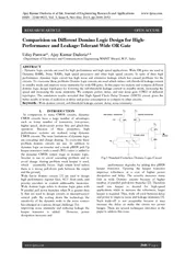
Int Journal of Engineering Research and Applications wwwijeracom ISSN 2248 9622 Vol 3 Issue 6 Nov Dec 2013 pp 2048 20 52 wwwijeracom ID: 90933

Int. Journal Engineering Research

Share:

Link:

Embed:

Download Presentation from below link

Download Pdf The PPT/PDF document "Ajay Kumar Dadoria et al" is the property of its rightful owner. Permission is granted to download and print the materials on this web site for personal, non-commercial use only, and to display it on your personal computer provided you do not modify the materials and that you retain all copyright notices contained in the materials. By downloading content from our website, you accept the terms of this agreement.


Presentation Transcript

Ajay Kumar Dadoria et al Int. Journal of Engineering Research and Applications www.ijera.com ISSN : 2248 - 9622, Vol. 3, Issue 6, Nov - Dec 2013, pp. 2048 - 20 52 www.ijera.com 2048 | Page Comparision o n Different Domino Logic Design f or High - Performance a nd Leakage - Tolerant Wide OR Gate Uday Panwar *, Ajay Kumar Dadoria** ( Department of Electronics and Communication Engineering MANIT Bhopal, M.P., India ABSTRACT - Dynamic logic cir cuits are used for high performance and high speed applications. Wide OR gates are used in Dynamic RAMs, Static RAMs, high speed processors and other high speed circuits. In spite of their high performance, dynamic logic circuit has high noise and extensiv e leakage which has caused problems for the circuits. To overcome these problems Domino logic circuits are used which reduce sub - threshold leakage current in standby mode and improve noise immunity for wide OR gates. In this paper we analyze and compare di fferent domino logic design topologies for lowering the sub - threshold leakage current in standby mode, increasing the speed and increasing the noise immunity. We compare power, delay, and unit noise gain (UNG) of different topologies. The simulation result s revealed that High Speed Clock Delay Domino (HSCD) circuit gives the better results in terms of reduction in delay and power consumption as compare to other circuits. Keywords - Wide domino circuit, sub - threshold leakage current, delay, noise immunity. I. INTRODUCTION In comparison to static CMOS circuits, dynamic CMOS circuits have a large number of advantages such as lower number of transistors, low - power, higher speed, short - circuit power free and glitch - free operation. Because of these properties, hi gh performance systems are realized using dynamic CMOS circuits. The main limitations of dynamic logic are cascading and charge sharing. To overcome these problem domino circuits are use. In addition to dynamic logic an inverter and a weak pMOS pull - Up kee per transistor (with a small (W/L) ratio) is added to the dynamic CMOS output stage in domino logic. Inverter is use to avoid cascading problem and to avoid charge sharing problem weak keeper is used, which essentially forces high output level unless th ere is a strong pull - down path between the output and the ground . Wide fan - in domino circuits [1] are used to design high performance register files, ALU front ends, and priority encoders in content addressable memories. Wide domino logic refers to domino logic gates with N parallel pull down branches when N is greater then 4; that are used to design circuits in microprocessor critical path. By scaling down the technology the sensitivity of the dynamic node to the noise sources has emerged as a serious des ign challenge. For improving noise immunity and reducing leakage the keeper transistor is added. However, power dissipation increases and Fig.1 Standard Footerless Domino Logic Circuit performance degrades by ad ding this pMOS keeper transistor. Upsizing the keeper transistor improves robustness at a cost of higher power dissipation and delay. The severity increases many fold in wide Domino circuits because of higher number of parallel pull - down branches [2]. Ther efore small size keeper is desired for high - speed applications while to increase the robustness, larger keeper is required. Thus, trade off exist between delay and power to improve noise and leakage immunity [3]. Such trade - off is not acceptable because it may increase the delay or make the circuit too power hungry. There are several techniques introduce in the paper to address this issue. RESEARCH ARTICLE OPEN ACCESS Ajay Kumar Dadoria et al Int. Journal of Engineering Research and Applications www.ijera.com ISSN : 2248 - 9622, Vol. 3, Issue 6, Nov - Dec 2013, pp. 2048 - 20 52 www.ijera.com 2049 | Page Fig. 2 Failure mechanism for 16 - in OR gate (FLDL) The rest of the paper is arranged as follows. Section II, studies five types of circuits that have been proposed in related literatures, standard footless domino logic, standard footed domino logic, conditional keeper domino logic, high speed domino logic, split domino logic and high speed clock delay domino logic. Sim ulation results of different methods and compare in section II . Conclusion in section III. II. PREVIOUS TECHNIQUE A. Standard Footless Domino Logic Circuit (SFLDL) The footless scheme [4] is characterized by the fact that discharge of dynamic node is faster. This property is exploited by the high - performance circuits. The circuit of the SFLD logic is shown in Fig1. Operation of Footless - Domino is as follows: During the pre - charge phase, i.e. when then clock (CLK) is LOW, the dynamic node is charged to V DD and the keeper transistor MP 2 turns ON to maintain the voltage of the dynamic node. During the evaluation mode, i.e. when the CLK goes HIGH, the dynamic node is either discharged to ground or remains HIGH depending on the inputs. The size of the keeper transi stor should be large enough to compensate for charge sharing problem and at the same time it should be small enough to reduce the contention between the keeper and the nMOS pull down transistor in the case the pull down network evaluates the dynamic node t o logic level zero. Otherwise, the pull down network and keeper transistor compete to drive the dynamic node to two opposite directions, this effect is called contention and this results in the degradation of speed. B. Standard Footed Domino Logic Circuit (SFDL) The footer nMOS transistor MN 2 is connected to the source of evaluation nMOS transistor to obtain the FDL [5] design which basically reduces the leakage current. The speed the SFDL is lower than the footless one because of the stacking effect, but the noise immunity is higher. Fig.3 shows the most conventional footed domino logic circuit. When clock is low, the dynamic node is pre - charged to V DD [7]. In this phase the footed transistor MN 2 is turned off, which reduces the leakage current. When clock goes high, footer transistor MN 2 is turned on. So, depending on incoming data to pull - down network the state of output node is obtained. Fig.3 standard footed domino logic circuit C. High Speed Domino Logic (HS) The circuit of the HS Domino logic is shown in Fig.4 [6]. In HS domino the keeper transistor is driven by a combination of the output node and a delayed clock. The circuit works as follows: At the start of the evaluation phase, when clock is high, MP 3 turns on and t hen the keeper transistor MP 2 turns OFF. In this way, the contention between evaluation network and keeper transistor is reduced by turning off the keeper transistor at the beginning of evaluation mode. After the delay equals the delay of two inverters, tr ansistor MP 3 turns off. At this moment, if the dynamic node has been discharged to Fig.4 High Speed Domino Logic ground, i.e. if any input goes high, the nMOS transistor MN 1 remains OFF. Thus the voltage at the gate of th e keeper goes to V DD - V th and not V DD causing higher leakage current though the keeper transistor[7]. On the other hand, if the dynamic node remains high during the evaluation phase (all inputs at „„0‟‟, standby mode), MN 1 turns on and pulls the gate of the keeper transistor. Thus keeper transistor will turn on to keep the dynamic node high, fighting the effects of leakage. Ajay Kumar Dadoria et al Int. Journal of Engineering Research and Applications www.ijera.com ISSN : 2248 - 9622, Vol. 3, Issue 6, Nov - Dec 2013, pp. 2048 - 20 52 www.ijera.com 2050 | Page D. Conditional Keeper Domino Logic (CKD) Conditional Keeper employs two keepers, small keeper and large keeper [8]. In this technique, the keeper device (PK) in conventional domino is divided into two smaller ones,PK1 and PK2. The keeper sizes are chosen such that PK=PK1+PK2 [9]. Such sizing insures the same level of leakage tolerance as the conventional gate but yet improving the speed. The circuit works as follows: in pre - charge phase when clock is low, the pull - up transistor is on, so the dynamic node starts being charge up to V DD . At the beginning of evaluation phase when clock is high pre - charge transistors and large keeper PK1 are of f. When all the inputs are at low logic level, i.e. in standby mode, the dynamic node after the delays of two inverters remains high, in this condition the output node of NAND gate goes low, this causes the large keeper PK1 to be turned on. The large keepe r is deployed after a delay for two inverters, to prevent erroneous discharge of the dynamic node when all inputs remain LOW. The small keeper PK2; however remain ON to compensate for charge leakage until PK1 is activated. E. Split Domino Logic (SDL) As m entioned before, there are many parallel branches in a large fan - in dynamic OR gate. When the dynamic node voltage remains at V DD , the nMOS pull - down branches cause a large amount of leakage current. The propagation delay is increased due the large parasit ic capacitive effect as this parasitic capacitance must be discharged to zero during evaluation. Split - domino is a very smart technique that by splitting the pull - down network into smaller groups improves the operation of the gate by using small size of ke eper in both Fig.5 Conditional Keeper Domino Logic Dynamic timing and strength variation of the CKD during the evaluation time situations [10]. Therefore, in theory we need two ke eper transistors with a width almost half as much as the conventional circuit. Fig.6 shows the 16 - bit domino OR gate split in two. The circuit overhead is not as much as it might look, as there are two static inverters in the conventional domino circuit in place of two and three input NAND gates and besides they can be implemented using minimum size transistors. The circuit overhead is almost the same as the conditional keeper technique. F. High Speed Clock Delay Domino Logic (HSCD) Another proposed circui t topology of High Speed Clock Delay Domino circuit[11] is shown in Fig.7. In this circuit footer transistor MN 1 is added to the tail of the evaluation network, which employs stacking effect. Thus the noise immunity improves. At the beginning of the evalu ation phase steady state voltage of N - FOOT node is uses to reduce leakage of the evaluation network. The circuit works as follow: Preacharge Mode: during the preacharge mode when clock is low precharge transistor is turned on which charge the dynamic node to V DD . in addition pMOS keeper transistor is turned on helping the precharge. MN 1 is also ON at the beginning of the evaluation phase which connects the N - FOOT node to ground. Furthermore, node GMN2 is low which is connected to the gate of MN 2 and thus MN 2 is OFF. After the delay equals to the delay of the two inverter (delay element), transistor MN 1 turns off. After the delay of an inverter, MN 1 turns off. In this case, the N - FOOT node voltage rises to an intermediate voltage level. To avoid any possibi lity of short circuit current in the precharge phase evaluation transistors are sized such that the DC voltage on GMN2 node does not exceed the threshold voltage of MN 2 . Evaluation mode: in evaluation mode clock is high. There is two possibility first when all the inputs are low (standby mode) and second when any input is high(active mode). Standby Mode: In standby mode, i.e. when all the inputs are at logic low level, nMOS footer transistor MN 1 is OFF at the Ajay Kumar Dadoria et al Int. Journal of Engineering Research and Applications www.ijera.com ISSN : 2248 - 9622, Vol. 3, Issue 6, Nov - Dec 2013, pp. 2048 - 20 52 www.ijera.com 2051 | Page Fig.6 Split Domino Logic Circuit beginning of the evaluation phase. Therefore, N - FOOT node voltage charges up to a DC voltage. This DC voltage reduces leakage of the evaluation network substantially resulting in significant leakage power reduction. Active Mode: When any o ne of the input switches from low to high, the N - FOOT node voltage increases at the beginning of the evaluation phase which turns on transistor MP3. Fig.7 High Speed Clock Delay Domino Logic Consequently, node GMN2 is charg ed to a voltage that is supplied by N - FOOT node voltage. Therefore, GMN2 voltage goes higher than the threshold voltage of MN 2 depending on the sizing of the transistors. Then at the onset of evaluation phase while the footer transistor MN 1 is OFF, nMOS tr ansistor MN 2 turns on which connects the dynamic node to ground. However the size of the MN 2 decides the amount of discharging current through MN 2 . After a delay equals to the delay of two inverters, N - FOOT node is connected to ground and the rest of evalu ation phase is accomplished through the footer transistor, MN 1 . When the dynamic node goes low, the output node becomes high, turning on MN 3 that leads to OFF MN 2 . However, the rest of evaluation phase (discharging of the dynamic node) completes through th e evaluation network and the footer transistor that is fully on. Here we have more degree of freedom for increasing speed or enhancing noise immunity. III. PERFORMANCE COMPARISON OF PRESENTED METHODES Simulations are performed in 65 nm technology at 2 GHz freq uency and V DD of 1 V. The fall/rise times of the waveforms were set to 1pS. Considering the application of wide OR gates delay, power dissipation and UNG(Unit Noise Gain) has been calculated for 8 input and 16 input OR gate to compare different topologies . For calculation of UNG [11], a pulse noise is applied to all inputs with amplitude which is a fraction of supply voltage and a pulse width equal to 30% of duty cycle. Then, the amplitude of the input noise pulse is increased until the amplitude of the r esulting output noise voltage is equal to that of the input noise signal. This noise amplitude is defined as UNG= Vin,Vnoise = Voutput Transient Analysis  Transient analysis shows a graph between inputs, outputs with respect to time axis. Fig.8 sh ows the waveform of inputs, outputs, clock and dynamic node voltage of 8 inputs OR gate based on proposed circuit and based on DCLCR logic style respectively. Fig. 8 Simulation results of 8 inputs DCLCD based OR gate Area: This is the Layout Diagram f or area Calculation of Fig.8 Layout Diagram Ajay Kumar Dadoria et al Int. Journal of Engineering Research and Applications www.ijera.com ISSN : 2248 - 9622, Vol. 3, Issue 6, Nov - Dec 2013, pp. 2048 - 20 52 www.ijera.com 2052 | Page TABLE I Result for 8 Input OR gate Dela y UN G Power dissipatio n EVALUATIO N DELAY (ps ) SFLD 1 1 1 1 SFD 1.07 1.01 .85 8.14 CKD 1.01 .94 1.02 14.40 HS .96 1.02 1.01 8.22 SD .94 .93 1.11 11.39 HSC D .93 3.1 1.02 13.80 TABLE II Result for 16 Input OR gate Delay UNG Power dissipation EVALU ATION DELAY (ps ) SFLD 1 1 1 1 SFD 1.09 1.03 0.87 17.54 CKD 1.05 0.9 1.05 11.96 HS 0.951 0.97 1.03 14.54 SD 0.921 0.95 1.25 17.98 HSCD 0.907 3.3 1.1 19.08 I. CONCLUSI ON In this paper, several domino logic circuit topologies were proposed for high - speed and leakage - tolerant design. High speed clock delayed (HSCD) domino method has the best performance among others. HSCD has a speed improvement of 9% as compared to SFLD and noise immunity also increases. HSCD method can be used for very high speed circuit. REFERENCES [1] L. T. Clarke, G. F. Taylor, “High fan - in circuit design,” IEEE Journal of Solid - State Circuits, vol. 31, Issue 1, January 1996, pp.91 - 96. [2] Fars had Moradi, TuanVuCao, ElenaI. Vatajelu, AliPeiravi, Hamid Mahmoodi, DagT.Wisland, “Domino logic designs for high - performance and leakage - tolerant applications,” Elsevier INTEGRATION, the VLSI journal, Issue 24 April 2012. [3] Farshad Moradi, AliPeirav i, Hamid Mahmoodi, “A New Leakage Tolerant Design for High Fan - in Domino circuits, ” 2004 IEEE . [4] B. - Y. Tsui, L. - F. Chin, “A com prehensive study of the FIBL of nanoscale MOSFETs,” IEEE Transactions on Electron Devices 51 (10) (2004) 1733 – 1735. [5] F. Assaderaghi, D. Sinitsky, S.A. Parke, J. Bokor, P. KO, C. Hu, “A dynamic - threshold MOSFET for ultra - low voltage operation,” Electron Devices Meeting Tech. Digest (1994) 809 – 812. [6] M.W. Allam, M.H. Anis, M.I. Elmasry, “High speed dynamic logic style for scaled - down CMOS and MTCMOS technologies,” in: Proceedings of the International Symposium on Low Power Electronics and Design , 2000, pp. 155 – 160. [7] M. H. Anis, M. W. Allam, and M. I. Elmasry, “Energy - efficient noise - tolerant dynamic styles for sca led - down CMOS and MTCMOS technologies,” IEEE Trans. Very Large Scale (VLSI) Syst., 2002. [8] A. Alvandpour, R.K. Krishnamurthy, K. Soumyanath, S.Y. Borkar, “A sub - 130 - nm conditional keeper technique,” IEEE Journal of Solid - State Circuits 37 (2002) 633 - 638 . [9] A. Alvandpour, R. Krishnamurthy, K. Soumayanath, ands. Borkar, “ A Low - Leakage Dynamic Multi Ported Register File in 0.13 µm CMOS ,” in proceedings of international Symposium on Low Power Electronics and Design, 2001, pp. 68 - 71. [10 ] Mohamed Elgebaly and Manoj Sachdev, “ A leakage Tolerant Energy Efficient Wide Domino Circuit Technique ” 2002 IEEE. [11] Farshad Moradi, Tuan VuCao, ElenaI. Vatajelu, Ali Peiravi, Hamid Mahmoodi, DagT.Wisland, “Domino logic designs for high - performanc e and leakage - tolerant applications,” INTEGRATION, the VLSI journal (2012).