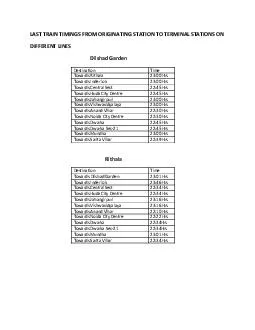
/
Last results on HARDROC 3 Last results on HARDROC 3

Last results on HARDROC 3 - PowerPoint Presentation

lindy-dunigan
lindy-dunigan . @lindy-dunigan
Follow
367 views
Uploaded On 2018-02-17

Last results on HARDROC 3 - PPT Presentation

OMEGA microelectronics group Ecole Polytechnique CNRSIN2P3 Palaiseau France OMEGA 19032014 3 rd generation chip for ILD Independent channels zero suppress I2C link IPNL ID: 632502

2014 hr3 data chip hr3 2014 chip data pll test power slave clock hit mode control consumption suppress tests

Share:

Link:

Embed:

Download Presentation from below link

Download Presentation The PPT/PDF document "Last results on HARDROC 3" is the property of its rightful owner. Permission is granted to download and print the materials on this web site for personal, non-commercial use only, and to display it on your personal computer provided you do not modify the materials and that you retain all copyright notices contained in the materials. By downloading content from our website, you accept the terms of this agreement.


Presentation Transcript

Slide1

Last results onHARDROC 3

OMEGA microelectronics group Ecole Polytechnique CNRS/IN2P3 , Palaiseau (France)

OMEGA,

19/03/2014Slide2

3rd generation chip for ILDIndependent channels (zero suppress)I2C link (@IPNL) for Slow Control parameters and triple voting

HARDROC3: 1st of the 3rd generation chip to be submittedanalog part: extension of the dynamicPLL: integrated to generate

fast clock internallySubmitted in Feb 2013 (SiGe 0.35µm), funded by AIDA, received end of June 2013Die size ~30 mm2 (6.3 x 4.7 mm2)Packaged in a QFP208HR3 will equip 2-3m RPC chambers

HR3 18/03/2014

HARDROC3

2Slide3

HR3 18/03/2014

SIMPLIFIED SCHEMATICS

3Slide4

4

Slow Control

HR3 18/03/2014

S

low control common features:Triple votingRead back of control bit (also when chip running)Slow control access:Classical shift registerI2C serial link

Write frame:

Read frame:

S

A

A

A

P

Slave address

Reg address

data

W

S

R

A

A

P

Slave address

data

S

A

A

P

Slave address

Reg address

W

Clock

Data

Master

Slave

1

Slave

2

Slave

3

Slave

x

Pb: Data

stuck

to 0

inside

the chip

(buffer

added

by OMEGA to output the data)

I2C

link

test

only

possible

with

chip

modification (FIB)

Test OK

Test OK

See

belowSlide5

5

Full FIB (2 cut + 1 strap) to bypass buffer on board HR3_01:Write and Read access with Chip ID: 0xE2 / Reg @: 0x73 /

WrData

: 0x83I2C Tests on FIB chipsHR3 18/03/2014

Test OK

FIB (1 cut) to isolate buffer HR3_03:Only Write access possible (no acknowledge)

Test OK

Other I2C tests:

Tests @ High/Low temperature

I2C @ 400Khz with 500pF on

Bidir

data portSlide6

HR3 18/03/2014

Analog Part: FSB Linearity

FSB0

FSB0: 5s noise limit= 15 fCFSB1FSB2

Up to 10 pC Up to 50 pC6Slide7

HR3 18/03/2014

SCURVE measurementspedestal

100

fC7Slide8

8

PLL can generate fast clock internally (40 MHz):Multiplication factor is (N+1) / N is a SC parameter (1 to 31)Output freq of PLL can go up to 80MHz (needed is 40-50 MHz)

Full chain tested with charge injected on one and readout

PLL measurementsHR3 18/03/2014

5MHz  40 MHz2,5MHz

 20 MHz

Tests OKSlide9

9

Lock time (Bias ON):Green = PowerOnD / Blue = Out_PLL

Time needed to have a stable clock = 230 + 30 = 260 µs

PLL measurementsHR3 18/03/2014Tlock

= 260 µsOther measurements:PLL jitter < 150 psSlide10

Digital: Memory mapping

Chip ID is the first to be outputted during readout (MSB first)

MSB of each word indicates type of data:

“1”: general data (Hit ch number and number of events)“0”: BCID + encoded dataA parity bit/wordUp to 9232 bits (577x16) during readout Example of number of bits during readout:

HR2

HR3

1 chn hit

160

48

8 chn hit

1280

272

4 chn hit @ same time

160

144

10 chn hit @ same time

160

336

HR3 18/03/2014

10Slide11

Digital: zero suppress

Zero suppress (only hit channels are readout): test OK

Roll

mode SC : test OK If RollMode = “0”  Backward compatibility with 2Gen ROC chips behaviorOnly the N first events are storedIf RollMode = “1”  3Gen ROC chips behaviourUse the circular memory mode

Only the N last events are stored“Noisy Evt” SC: 64 triggers => Noisy event => no data stored : test OK“ARCID” SC (Always Read Chip ID): test OKIf ARCID = 0  Backward compatibility: No

event  No readoutIf ARCID= 1  New

behavior: No event  Read CHIP ID

HR3 18/03/2014

Signal

injected

only

in

ch

20 and 43

11Slide12

12

Power consumption

OMEGA ROC CHIPS

Power supplyHR3 With Clk from LVDS(Slow clock 5M + 40M)Consumption in µW / channelHR2 With Clk from LVDS(Slow clock 5M + 40M)Consumption in µW / channel

PowerOnA (Analog)16501325Only PowerOnADC (OTA)00Only PowerOnDAC

5550Only PowerOn D

72550

Power-On-All2430

1425

Power-On-All

@ 0,5%

duty

cycle

12,2

7,5

Power consumption in ILC mode:

Power measured on

AlimChip

over 1 Ohm

resistor

Buffer/SSH/

Widlar

/

OtaQ

/

OtaFSB

/Temperature OFF

Pll/FastClock

LVDS = 0/1 if clocks from LVDS else 1/0 EnPllOut / testOtaQ / ValdSS are disabledStartAcq OnNotes:Analog: increase due to extended dynamic rangeDigital: increase due to

zero suppress

If the PLL is activated, +3% on the power consumptionSlide13

Good analog performance: dynamic range extended up to 50 pCPLL alternative for fast clock Preliminary good digital performanceZero suppress, roll mode, ARCID mode, Noisy

evt mode tested successfully on testboardExternal trigger available to be able to check the status of each channelSlow control:Classic shift register, Triple voting and Read back are OKI2C problem understood and testedNext stepsMore intensive tests on zero suppress and analog part (multiple channels)

Production

run expected end 20142-3m long RPC chambers to be built and equipped with HR3 in 2015Possible improvements: PLL start boost, power consumptionHR3 18/03/2014

Summary and next steps13