/
 Manufacturing Defects Manufacturing Defects  Manufacturing Defects Manufacturing Defects

Manufacturing Defects Manufacturing Defects - PowerPoint Presentation

lindy-dunigan
lindy-dunigan . @lindy-dunigan
Follow
343 views
Uploaded On 2020-04-04

Manufacturing Defects Manufacturing Defects - PPT Presentation

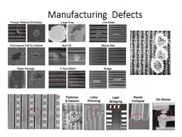
Relative size of contamination Resistive open due to unfilled via R Madge et al IEEE DampT 2003 Particle embedded between layers Even if there isnt a complete short or open resistance and capacitance variations can lead to trouble ID: 775349

air process contaminants surface air process contaminants surface particles wafer water device cleanroom area cleaning clean chemical size materials

Share:

Link:

Embed:

Download Presentation from below link

Download Presentation The PPT/PDF document " Manufacturing Defects Manufacturing Def..." is the property of its rightful owner. Permission is granted to download and print the materials on this web site for personal, non-commercial use only, and to display it on your personal computer provided you do not modify the materials and that you retain all copyright notices contained in the materials. By downloading content from our website, you accept the terms of this agreement.


Presentation Transcript

Slide1

Manufacturing Defects

Slide2

Manufacturing Defects

Relative size of contamination

Slide3

Resistive open due to unfilled via [R. Madge et al., IEEE D&T, 2003]

Particle embedded between layers

Slide4

Even if there isn’t a complete short or open, resistance and capacitance variations can lead to trouble

Chip temperature map

Slide5

Defect are of two main types:

Not every spot defect leads to structural or parametric damageActual damage depends on location and size (relative to feature size)

Global or gross-area defects are due to: Scratches (e.g., from wafer mishandling) Mask misalignment over- and under-etching

Local or spot defects are due to:

Imperfect process (e.g., extra or missing material)

Effects of airborne particles

Slide6

Excess-Material and Pinhole Defects

Extra-material defects are modeled as circular areas

Pinhole defects are tiny breaches in the dielectric between conducting layers

From:

http://www.see.ed.ac.uk/research/IMNS/papers/IEE_SMT95_Yield/IEEAbstract.html

Slide7

Defect Size Distribution

Sample random defect size

distribution, assuming 0.3 defects per cm2

From: http://www.design-reuse.com/articles/10164/model-based-approach-allows-design-for-yield.html

f

(

x) =

kx–p for xmin < x < xmax 0 otherwise

x

= Defect diameter

f

(x) = Defect density

k = Normalizing constant

p

is typically in [2.0, 3.5]

Slide8

The Bathtub Curve

Many components fail early on because of residual or latent defectsComponents may also wear out due to aging (less so for electronics)In between the two high-mortality regions lies the useful life period

Time

Failure rate

Infant mortality

End-of-life wearout

Useful life

(low, constant failure rate)

Mechanical

Electronic

Primarily due to latent defects

l

Slide9

Survival Probability of Electronic Components

From:

http://www.weibull.com/hotwire/issue21/hottopics21.htm

Infant mortality

Time in years

Percent of parts still working

No significant

wear-out

Bathtub curve

Slide10

From:

http://www.weibull.com/hotwire/issue21/hottopics21.htm

Time in years

Percent of parts still working

Burn-in and stress tests are done in accelerated form

Difficult to perform on complex and delicate ICs without damaging good parts

Expensive “ovens” are required

Burn-in and Stress Testing

Slide11

Burn-in Oven Example

From: http://www.goldenaltos.com/environmental_options.html

Slide12

Cause of contamination

Slide13

Forms and types of contaminants

Slide14

Effects of contaminants

Slide15

5 major classes of contaminants

Particles

Metallic ions

Chemicals

Bacteria

Airborne molecular contaminants (AMCs)

Slide16

1. Particles

Small feature size and thinness of deposited layer of semiconductor devices make them vulnerable to all kinds of contaminations

Particle size must be 10 times smaller than the minimum feature size e.g. 0.30

m feature size device is vulnerable to 0.03m diameter particles

Killer defects

Particles present in a critical part of the device and destroy its functioning

Crystal defects and other process induced problems

If contaminants present in less sensitive area

 do not harm the device

Slide17

Relative size of contamination

Slide18

Slide19

Slide20

Slide21

Slide22

Slide23

2. Metallic ions

Controlled resistivity is required in semiconductor wafers; in N, P and N-P junction

The presence of a small amount electrically active contaminants in the wafer could results in

Change device electrical characteristics

Change performance

Reliability parameters

The contaminants that cause this problem is called Mobile Ionic Contaminants (MIC)

Metal atoms that exist in an ironic form in the wafer

Slide24

MIC is highly mobile: metallic ions can move inside the device even after passing electrical testing and shipping  cause device failsMIC must be in < 1010 atoms/cm2Sodium is the most common MIC especially in MOS devices  look for low-sodium-grade chemicals

Trace Metal Parts per Billion (ppb) Impurity

Sodium

50

Potassium

50

Iron

50

Copper

60

Nickel

60

Aluminum

60

Manganese

60

Lead

60

Zinc

60

Chlorides

1000

Slide25

3. Chemicals

Unwanted chemical contamination could occur during process chemicals and process water

This may result in:

Unwanted etching of the surface

Create compound that cannot be removed from the device

Cause non-uniform process

Chlorine is the major chemical contaminant

Slide26

Liquid chemicals in semiconductor industries

Slide27

4. Bacteria

Can be defined as organisms that grow in water systems or on surfaces that are not cleaned regularly

On semiconductor device, bacteria acts as particulate contamination or may contribute unwanted metallic ions to the device surface

Slide28

5. Airborne molecular contaminants (AMCs)

AMCs- fugitive molecules that escape from process tools, chemical delivery systems, or are carried out into a fabrication area on materials or personnel

AMCs: gasses, dopants, and process chemicals used in fabrication area e.g. oxygen, moisture, organics, acids, bases etc..

Problems:

Harmful to process that requires delicate chemical reactions such as the exposure of photoresist in the patterning operations

Shift etch rates

Unwanted dopants that shift device electrical parameters

Change the wetting characteristics of etchants leading to incomplete etching

Slide29

The effects of contamination on semiconductor devices

Device processing yield

- contaminants may change the dimensions device parts

- change cleanliness of the surfaces

- pitted layers

 reduce overall yield through various quality checks

Device performance

- This may due to the presence of small pieces of contamination that is not detectable during quality checks

- may also come from unwanted chemicals or AMCs in the process steps

 alter device dimensions or material quality

- high amount of mobile ionic contaminants in the wafer can change the electrical performance of the device

Slide30

Air

Normal air contains contaminants

 must be treated before entering a cleanroom

Major contaminant is airborne particles; particulates or aerosols

They float and remain in air for long period of time

Air cleanliness levels of cleanroom is determined by the

Particulate diameters

Density in air

Federal standard 209E: class number of the air in the area

Number of particles 0.5m or larger in a cubic foot of air

In normal city with smoke, smog and fumes can contains up to 5 million particles per cubic foot: class number 5 million

Slide31

Federal 209E:Specify cleanliness level down to class 1 levels

Slide32

Environment Class numberMaximum particle size (m)Projected-256 merit 0.01<< 0.1Mini environment0.1< 0.1ULSI fab10.1VLSI fab100.3VLF station1000.5Assembly area1000-10 0000.5House room100 000Outdoors> 500 000

Typical class numbers for various environments

Slide33

Air cleanliness standard 209E

Slide34

Clean air strategies

Clean workstation

Tunnel design

Total cleanroom

Mini-environments

Slide35

Production facility

Clean room strategy

Fabrication area consists of a large room with workstations (called hoods) arranged in rows so that the wafers could move sequentially through the process without being exposed to dirty air

Use high-efficiency particulate attenuation (HEPA) filters or ultra-low-particle (ULPA) filters

Allow passage of large volumes of air at low velocity

Low velocity contributes to the cleanliness of the hood by not causing air currents, and also for operators comfort

HEPA and ULPA filters efficiency: 99.9999+ % at 0.12micron particle size

Typical flow 90-100

ft

/min

Slide36

HEPA and ULPA filters mounted on a clean hood

Vertical laminar flow (VLF)

 air leave the system in a laminar pattern, and at the work surface, it turns and exits the hood

Horizontal laminar flow (HLF)  HEPA filter is placed in the back of the work surface

Both VLF and HLF stations keep the wafer cleans:

Filtered air inside the hood

Cleaning action inside is the slight positive pressure built up in the station  prevent airborne dirt from operators and from aisle area from entering the hood

Slide37

Cross-section of VLF fixed with HEPA/ULPA filter

HEPA filter

Slide38

Cleanroom construction

Primary design is to produce a sealed room that is supplied with clean air, build with materials that are non contaminating, and includes the system to prevent accidental contamination from the outside or from operators

All materials must be non-shedding including wall covering, process station materials and floors coverings

All piping holes are sealed and all light fixtures must have solid covers

Design should minimise flat surfaces that can collect dust

Stainless steel is favourable for process stations and work surfaces

Slide39

Slide40

Slide41

Fabrication area with gowning area, air showers, and service aisle

Slide42

Cleanroom elements:

Adhesive floor mats

At every entrance to pull off and holds dirt adhered at the bottom of the shoes

Gowning area

Buffer between cleanroom and the plant

Always supply with filtered air from ceiling HEPA filters

Store cleanroom apparel and change to cleanroom garments

Air pressure

Highest pressure in cleanroom, second highest in gowning area and the lowest in factory hallways

Higher pressure in cleanroom causes a low flow of air out of the doors and blow airborne particle back into the dirtier hall way

Slide43

Air showers

Air shower is located between the governing room and the cleanroom

High velocity air jets blow off particles from the outside of the garments

Air shower possesses interlocking system to prevent both doors from being opened at the same time

Service bay

Semi-clean area for storage materials and supplies

Service bay has Class 1000 or class 10 000

Bay area contains process chemical pipes, electrical power lines and cleanroom materials

Critical process machines are backed up to the wall dividing the cleanroom and the bay

 allows technician to service the equipment from the back without entering the cleanroom

Slide44

Double-door-pass-through

Simple double-door boxes or may have a supply of positive-pressure filtered air with interlocking devices to prevent both doors from being opened at the same time

Often fitted with HEPA filters

Static control

Slide45

Static charge

 attracts smaller particles to the wafer

The static charge may build up on wafers, storage boxes, work surfaces and equipment

May generate up to 50 000V static charge  attract aerosols out of the air and personal garment  contaminate the wafers

Particles held by static charge is hard to remove using a standard brush or wet cleaning system

Most static charge is produced by triboelectric charging

2 materials initially in contact are separated

1 surface possesses positive charge because it losses electron

1 surface becomes negative because it gains electron

Slide46

How particles are attracted to charge particles

Slide47

Slide48

Electrostatic Discharge (ESD):

rapid transfer of electrostatic charge between two objects, usually resulting when two objects at different potentials come into direct contact with each other. 

ESD can also occur when a high electrostatic field develops between two objects in close proximity. 

Control static

Prevent charge build up

Use antistatic materials in garments and in-process storage boxes

Apply antistatic solution on certain walls to prevent charge build up- not use in critical station due to possible contamination

Use discharge technique

Use ionisers and grounded static-discharge

Slide49

Eliminating static charge:

Air ioniser – neutralise nonconductive materials

Grounding of conducting surfaces

Increasing conductivity of materials

Humidity control

Surface treatment with topical

antistatic

solutions

Slide50

Shoe cleaners

Removal of dirt from the sides of shoes and shoes cover

Rotating brushes to remove the dirt

Typical machines feature an internal vacuum to capture the loosened dirt, and bags to hold the dirt for removal from the area

Glove cleaners

Discard gloves when they are contaminated or dirty or after every shift

Some fabrication areas use glove cleaners that clean and dry the gloves in an enclosure

Slide51

Typical cleanroom garments

Slide52

Slide53

Slide54

Cleanroom personnel

Even after shower and sitting: 100,000 – 1,000,000 particles/minute

Increase dramatically when moving e.g. generate 5 million particles/min with movement of 2 miles/

hr

Example of human contaminants:

Flakes of dead hair

Normal skin flaking

Hair sprays

Cosmetics

Facial hair

Exposed clothing

Slide55

Process water

During fabrication process

Repeated chemical etch and clean

Water rinse is essential after etching/ cleaning step

 several hours in the whole system

Unacceptable contaminants in normal city water

Dissolves minerals

Particles

Bacteria

Organics

Dissolved O

2

Silica

Slide56

Dissolve minerals

Comes from salt in normal water Na

+

Cl

-

Can be removed by reverse osmosis (RO) and ion exchange systems

Remove electrically active ions

 change water from conductive medium to resistive medium

It is a must to monitor resistivity of all process water in the fabrication area

Need to obtain between 15-18 M

Remove contaminants

Solid particles: sand filtration, earth filtration, membrane

Bacteria: sterilise using UV radiation and filter out the particles

Organics (plant &

fecal

materials): carbon bed filtration

Dissolved O

2

& CO

2

: force draft

decarbonators

and vacuum

degasifiers

Slide57

Cleaning cost is a major operating costCertain acceptable water quality: recycle in a water system for clean upToo dirty water: treated and discharge from plant

Resistivity Ohms-cm 25Dissolved solids (ppm)18,000,0000.027715,000,0000.033310,000,0000.05001,000,0000.500100,0005.0010,00050.00

Resistivity of water vs concentration of dissolved solids (ppm)

Slide58

Process chemicals

Highest purity of acids, bases and solvents are used for etching and cleaning wafers and equipment

Chemical grades:

Commercial

Reagent

Electronic

Semiconductor

Main concerns: metallic mobile ionic contaminants (MIC)

 must be < 1 ppm

To date, can obtain chemicals with 1ppb MIC

Check assay no e.g. assay 99.9% purity

Other steps:

Clean inside containers

Use containers that do not dissolve

Use particulate free labels

Place clean bottles in bags before shipping

Slide59

Process gasses

Semiconductor fabrication uses many gases:

Air separation gases: O

2

, N

2

, H

2

Specialty gases: arsine and carbon tetrafluoride

Determination of gas quality

Percentage of purity

Water vapour content

Particulates

Metallic ions

Semicnductor

fabrication requires extremely high purity process gasses for oxidation, sputtering, plasma etch, chemical vapour deposition (CVD), reactive ion gas, ion implantation and diffusion

Slide60

If gas is contaminated, wafer properties could be altered due to chemical reaction

Gas quality is also shown in assay no; 99.99-99.999999. The highest quality is called “six 9s pure”

Slide61

Requirements for Si wafer cleaning process

Effective removal of all types of surface contaminants

Not etching or damaging Si and SiO

2

Use of contamination-free and volatilisation chemicals

Relatively safe, simple, and economical for production applications

Ecologically acceptable, free of toxic waste products

Implementable by a variety of techniques

Slide62

Wafer surface cleaning

4 general types of contaminants:

Particulates

Organic residues

Inorganic residues

Unwanted oxide layers

Wafer cleaning process must

Remove all surface contaminants

Not etch or damage the wafer surface

Be safe and economical in a production setting

Be ecologically acceptable

2 primary wafer conditions:

Front end of the line (FEOL)

Back end of the line (BEOL)

Slide63

FEOL

Wafer fabrication steps used to form the active electrical components on the wafer surface

Wafer surface especially gate areas of MOS transistors, are exposed and vulnerable

Surface roughness: excessive roughness results in degradation of device performance and compromise the uniformity

Electrical conditions of bare surface

Metal contaminants

Na, Ni, Cu, Zn, Fe

etc

: cleaning process need to reduce the concentration to < 2.5 x 10

9

atoms /cm

2

Al and Ca contaminants: need to reduce to 5 x 10

9

atoms/cm

2

level

Slide64

Typical FEOL cleaning process steps

Particle removal (mechanical

General chemical clean (such as sulphuric acid/H

2

/O

2

Oxide removal (typically dilute HF)

Organic and metal removal

Alkali metal and metal hydroxide removal

Rinse steps

Wafer drying

Slide65

BEOL

Main concerns: particles, metals, anions, polysilicon gate integrity, contact resistance, via holes cleanliness, organics, numbers of shorts and opens in the metal system

Slide66

Particulate removal

Spray: blow off the water surface using spray of filtered high pressure nitrogen from a hand-held gun located in the cleaning station

In fabrication area/small particles: nitrogen guns are fitted with ioniser that strip static charges from the nitrogen stream and neutralise the wafer surface

Wafer scrubbers-combination of brush and wafer surface.

High pressure water cleaning

Slide67

Organic residues

Organic residues- compounds that contain carbon such as oils in fingerprints

Can be removed in solvent baths such as acetone, alcohol or TCE

Solvent cleaning is avoided:

difficulty of drying the solvent completely

Solvents always contain some impurities that may cause contamination

Slide68

Inorganic residues

Organic residues- do not contain carbon e.g. HCl and HF from steps in wafer processing

Slide69

Chemical cleaning solutions

For both organic and inorganic contaminants

General chemical cleaning

Sulphuric acid

Hot sulphuric acid with added oxidant

Also a general photoresist stripper

H

2

SO

4

is an effective cleaner in 90-125C  remove most inorganic residues and particulates from the surface

Oxidants are added to remove carbon residues

Chemical reaction converts C to CO

2

Typical oxidants: hydrogen peroxide (H

2

O

2

), ammonium persulfate [(NH

4

)

2

S

2

O

8

]

Nitric acid (HNO

3

), and ozone (O

2

)

Slide70

RCA clean

RCA clean- H

2

O

2

is used with some base or acid

Standard clean 1 (SC-1)

Solution of water, hydrogen peroxide, ammonium hydroxide = 5:1:1, 7:2:1, heated to 75-85

C

SC-1 removes organic residues and set up a condition for desorption of trace metals from the surface

Oxide films keep forming and dissolving

SC-2

Solution of water, hydrogen peroxide and hydrochloric acid = 6:1:1 to 8:2:1, 75-85

C

Remove alkali ions and hydroxides and complex residual metals

Leave a protective oxide layer

Slide71

Order of SC-1 and SC-2 can be reversed

If oxide-free surface is required, HF step is used before, in between, or after the RCA cleans