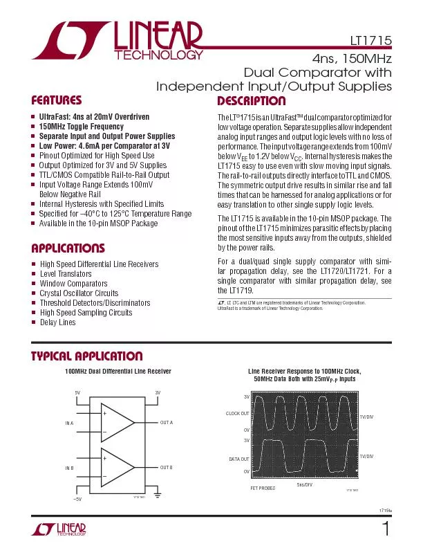
/
The LT1715 is an UltraFast The LT1715 is an UltraFast

The LT1715 is an UltraFast - PDF document

lois-ondreau
lois-ondreau . @lois-ondreau
Follow
409 views
Uploaded On 2016-11-03

The LT1715 is an UltraFast - PPT Presentation

LT1715 1 LT LTC and LTM are registered trademarks of Linear Technology Corporation UltraFast is a trademark of Linear Technology Corporation UltraFast 4ns at 20mV Overdriven 150MHz Toggle Frequ ID: 484102

LT1715 1 LTC and LTM

Share:

Link:

Embed:

Download Presentation from below link

Download Pdf The PPT/PDF document "The LT1715 is an UltraFast" is the property of its rightful owner. Permission is granted to download and print the materials on this web site for personal, non-commercial use only, and to display it on your personal computer provided you do not modify the materials and that you retain all copyright notices contained in the materials. By downloading content from our website, you accept the terms of this agreement.


Presentation Transcript

LT1715 1 The LT1715 is an UltraFast’ dual comparator optimized for low voltage operation. Separate supplies allow independent performance. The input voltage range extends from 100mV to 1.2V below V. Internal hysteresis makes the LT1715 easy to use even with slow moving input signals. The rail-to-rail outputs directly interface toTTL and CMOS. times that can be harnessed for analog applications or for The LT1715 is available in the 10-pin MSOP package. The pinout of the LT1715 minimizes parasitic effects by placing lar propagation delay, see the LT1720/LT1721. For a , LT, LTC and LTM are registered trademarks of Linear Technology Corporation. UltraFast is a trademark of Linear Technology Corporation. UltraFast: 4ns at 20mV Overdriven 150MHz Toggle Frequency Separate Input and Output Power Supplies Low Power: 4.6mA per Comparator at 3V Pinout Optimized for High Speed Use Output Optimized for 3V and 5V Supplies TTL/CMOS Compatible Rail-to-Rail Output Internal Hysteresis with Speci“ ed Limits Speci“ ed for …40°C to 125°C Temperature Range Available in the 10-pin MSOP Package High Speed Differential Line Receivers Level Translators n Window Comparators n Crystal Oscillator Circuits Threshold Detectors/Discriminators n High Speed Sampling Circuits Delay Lines + + INA5V3V 5ns/DIV1V/DIVCLOCK OUTDATA OUT0V0V3V3V FET PROBES LT1715 2 Supply Voltage +V to GND .............................................................7V ..........................................................13.2V +V ..........................................................13.2V to GND .........................................…13.2V to 0.3VInput Current (+IN, …IN) .......................................±10mAOutput Current (Continuous) ...............................±20mAOperating Temperature Range (Note 2) LT1715C ...............................................…40°C to 85°C LT1715I ................................................…40°C to 85°C LT1715H ............................................…40°C to 125°CSpeci“ ed Temperature Range (Note 3) LT1715C ...................................................0°C to 70°C LT1715I ................................................…40°C to 85°C LT1715H ............................................…40°C to 125°CJunction Temperature ...........................................150°CStorage Temperature Range ...................…65°C to 150°CLead Temperature (Soldering, 10 sec) ..................300°C (Note 1) 2+IN A…IN AVEE10VCC+VSOUT AOUT BTOP VIEWMS PACKAGE10-LEAD PLASTIC MSOP B SYMBOLPARAMETERCONDITIONSMINTYPMAXUNITSInput Supply Voltage 2.712VOutput Supply Voltage 2.76VInput Voltage Range(Note 5) … 0.1V … 1.2VInput Trip Points(Note 6) LT1715C, LT1715I LT1715H ll Input Trip Points(Note 6) LT1715C, LT1715I LT1715H ll …61.8mVmV LEAD FREE FINISHTAPE AND REELPART MARKINGPACKAGE DESCRIPTIONSPECIFIED TEMPERATURE RANGELT1715CMS#PBFLT1715CMS#TRPBFLTVQ10-Lead Plastic MSOP0°C to 70°CLT1715IMS#PBFLT1715IMS#TRPBFLTVV10-Lead Plastic MSOP…40°C to 85°CLT1715HMS#PBFLT1715HMS#TRPBFLTVV10-Lead Plastic MSOP…40°C to 125°CConsult LTC Marketing for parts speci“ ed with wider operating temperature ranges.Consult LTC Marketing for information on non-standard lead based “ nish parts. http://www.linear.com/leadfree/ For more information on tape and reel speci“ cations, go to: http://www.linear.com/tapeandreel/ The l denotes the speci“ cations which apply over the full operating temperature range, otherwise speci“ cations are at T = 5V, V = …5V, +V = 5V, V = 1V, C = 10pF, V = 20mV, unless otherwise speci“ ed. LT1715 3 The l denotes the speci“ cations which apply over the full operating temperature range, otherwise speci“ cations are at T = 5V, V = …5V, +V = 5V, V = 1V, C = 10pF, V = 20mV, unless otherwise speci“ ed. SYMBOLPARAMETERCONDITIONSMINTYPMAXUNITSInput Offset Voltage(Note 6) LT1715C, LT1715I LT1715H ll 0.42.5Input Hysteresis Voltage(Note 6) LT1715C, LT1715I LT1715H ll 3.56TInput Offset Voltage Drift 10µV/°CInput Bias Current LT1715C, LT1715I LT1715H ll …2.50Input Offset Current LT1715C, LT1715I LT1715H ll 0.20.6CMRRCommon Mode Rejection Ratio(Note 7) LT1715C, LT1715I LT1715H ll 70dBPSRRPower Supply Rejection Ratio(Note 8) 6580dBVoltage Gain(Note 9)Output High VoltageI … 0.4VOutput Low VoltageI 0.4VMaximum Toggle Frequency(Note 10)150MHzPropagation DelayV = 5V, V = …5V LT1715C, LT1715I LT1715H ll = 20mV, V = 5V, V = 0V4.4ns = 20mV, V = 3V, V LT1715C, LT1715I LT1715H ll 4.86.5Propagation DelayV = 5mV, V Propagation Delay Skew(Note 13) Between t 0.51.5nsDifferential Propagation Delay(Note 14) Between Channels 0.31nsOutput Rise Time10% to 90%2nsOutput Fall Time90% to 10%2nsJITTEROutput Timing JitterV = 50 tf = 20MHz (Note 15) t = 5V, V = …5V LT1715C, LT1715I LT1715H ll = 3V, V = 0V LT1715C, LT1715I LT1715H ll 0.91.6 = 5V, V = …5V LT1715C, LT1715I LT1715H ll …2.9mA = 3V, V = 0V LT1715C, LT1715I LT1715H ll …2.4mA = 5V, V = …5V LT1715C, LT1715I LT1715H ll 4.67.5 = 3V, V = 0V LT1715C, LT1715I LT1715H ll 3.76 LT1715 4 Input Offset and Trip Voltagesvs Supply VoltageInput Offset and Trip Voltagesvs Temperaturevs Temperature SUPPLY VOLTAGE, V4.05.03.03.54.55.56.0 TRIP+ OS TRIP… A = 25°CVVEE = GND …202060100 …6004080120 TRIP+ OS TRIP… S = VCC = 5VVCM = 1VVEE = …5V 2575…25050100125 4.0COMMON MODE INPUT VOLTAGE (V) S = VCC = 5VVEE = …5V The LT1715C is guaranteed functional over the operating range of The LT1715C is guaranteed to meet speci“ ed performance from 0°C to 70°C. The LT1715°C is designed, characterized and expected to meet speci“ ed performance from …40°C to 85°C but is not tested or QA sampled at these temperatures. The LT1715I is guaranteed to meet speci“ ed performance from …40°C to 85°C. The LT1715H is guaranteed to meet speci“ ed performance from …40°C to 125°C. Thermal resistances vary depending upon the amount of PC board is speci“ ed for a 2500mmcopper attached to Pin 5. Thermal performance can be improved beyond the given speci“ cation by using a 4-layer board or by attaching more metal The LT1715 comparator includes internal hysteresis. The trip direction. The offset voltage is de“ ned as the average of V = 5V, = …5V and is de“ ned as the change in offset voltage measured from = 3.8V, divided by 8.9V. de“ ned as the worst of: the change in offset voltage from V = 6V) divided by 6V.which to measure gain. Proper operation of internal circuity is ensured by Maximum toggle rate is de“ ned as the highest frequency at supply.low values of overdrive. The LT1715 is 100% tested with a 100mV step Propagation Delay Skew is de“ ned as: Differential propagation delay is de“ ned as the larger of the two:the other channel can increase the output jitter. See Channel Interactions in Applications Information. Speci“ cation above is with one channel active only. LT1715 5 vs Temperaturevs Supply Voltagevs Differential Input Voltagevs Temperaturevs Supply VoltageOutput Low VoltageOutput High Voltagevs Toggle Frequency …4…3…2…105 A = 25°CVCC = +VS = 5VVEE = …5V …25050 75100125 CC = +VS = 5VVEE = …5V SUPPLY VOLTAGE, VCC = +VS (V)0…4…3SUPPLY CURRENT PER COMPARATOR (mA)3624510…1…254136ICC7 A = 25°CVEE = GND S, OUTPUT HIGH S, OUTPUT LOW EE, OUTPUT LOW EE, OUTPUT HIGH OUTPUT SINK CURRENT (mA)0OUTPUT VOLTAGE (V)0.30.40.5160.104812 20125°C CC = +VS = 5V, UNLESS OTHERWISE NOTEDIN = …10mV +VS = 2.7V OUTPUT SOURCE CURRENT (mA)0OUTPUT VOLTAGE RELATIVE TO +VS (V)…0.3…0.2161715 G08…0.4…0.5…0.64812 20 +VS = 2.7V CC = +VS = 5V, UNLESS OTHERWISE NOTEDIN = 10mV 1252252575 30 A = 25°CVIN = ±50mV SINUSOID+VS = VCC = 5VVEE = GND LOAD = 20pF LOAD = 10pF LOAD = 0pF OUTPUT TOGGLINGVALIDTOGGLING 0PROPAGATION DELAY (ns)30501715 G10 102040 A = 25°CVSTEP = 100mVCLOAD = 10pF CC = +VS = 3VVEE = 0V CC = +VS = 5VVEE = …5V PDLH …25050 75100125 PDLHVSTEP = 100mVCLOAD = 10pF CC = +VS = 3VVEE = 0V CC = +VS = 5VVEE = …5V 4.05.03.03.54.55.56.0 A = 25°CVSTEP = 100mVOVERDRIVE = 20mVLOAD = 10pF EE = GND EE = …5VSUPPLY VOLTAGE, +VS = VCC OR V+ (V) LT1715 6 (Pin 5): Negative Supply Voltage for Input Stage and Positive Supply Voltage for Output Stage. Positive Supply Voltage for Input Stage.Maximum Toggle RateSine Wave Driving 10pF 102030505152545 A = 25°CVIN = ±50mV SINUSOID+VS = VCC = 5VVEE = GND OUTPUT LOAD CAPACITANCE (pF)0PROPAGATION DELAY (ns)3050 102040 A = 25°CVSTEP = 100mVOVERDRIVE = 20mVS = VCC = 5VVEE = …5V (tPDLH) PDHL) 2.5ns/DIV1715 G18NA25mVP-P5V0V 20mV/DIV1V/DIVOUT AFET PROBESVCC = 5VVEE = …5V+VS = 5VVCM = 0V Maximum Toggle RateMaximum Toggle Ratevs TemperatureMaximum Toggle Ratevs Supply Voltage 10100 A = 25°C+VS = VCC = 5VVEE = GNDCLOAD = 10pFTEMPERATURE (°C)…5050TOGGLE FREQUENCY (MHz)7011013015025019005075210230170…2525100125 A = 25°CVIN = ±50mV SINUSOID+VS = VCC = 5VVEE = …5VCLOAD = 10pFRLOAD = 500 +VS = VCC SUPPLY VOLTAGE (V)2TOGGLE FREQUENCY (MHz)15017520061715 G1512510050345 75250225 1V TO +VS … 1V A = 25°CVIN = ±50mV SINUSOIDVEE = GNDCLOAD = 10pF 20% TO 80% OF +VS LT1715 7 Test Circuit … … … 1/2 LT1715 BANDWIDTH-LIMITED TRIANGLE WAVE 100k2.4k10nF1µF0.15µF1/2 LT16381/2 LT1638100k100k200k10k 10k1000× VHYST1000× VTRIP+1000× VTRIP…1000× VOS0.1µF5050kVCMVCC … 1/2 LT11121µF NOTES: LT1638, LT1112, LTC203s ARE POWERED FROM ±15V. 200k PULL-DOWN PROTECTS LTC203 LOGIC INPUTS WHEN DUT IS NOT POWERED 14 11 3 6 LT1715 8 Response Time Test Circuit + …100mV…5VPULSEIN0V 0V 501N57114001302550+Vs … VCMVCC … VCMVEE … VCM …VCM50k DUT1/2 LT1715 250.1µF× SCOPE PROBE(CIN  10pF)0.01µF FOR FALLING EDGE, REVERSE LT1719 INPUTS LT1715 9 Power Supply Con“ gurationsThe LT1715 has separate supply pins for the input and exible operation, accommodating logic. Of course, a single 3V/5V supply may be used by guration: 2.7V  (V 2.7V  (+V (+Vmost applications will use it that way. Figure 1 shows three gurations. The “ nal one is uncommon, but input stage is run from …5.2V and ground while the output to 3V. Conversely, V may Input Voltage ConsiderationsThe LT1715 is speci“ ed for a common mode range of …100mV to 3.8V when used with a single 5V supply. A to 1.2V below Vone input is within the common mode limit, the other the correct polarity. mode limit, the internal PN diode formed with the substrate input and the negative rail can speed uprecovery from mode limit, phase reversal protection circuitry prevents However, the offset and hysteresis in this mode will increase dramatically, to as much as 15mV each. The input bias When one input signal goes above the common mode range the input stage will remain biased and the comparator will maintain correct output polarity. Above this voltage, the input stage current source will saturate completely and the ESD protection diode will forward conduct. Once the Figure 1. Variety of Power Supply Con“ gurations +VEEVCC2.7V TO 6V+VSGNDSingle Supply 5VInput, 3V Output Supplies +VEEVCC12V5V+VSGND12V Input, 5V Output Supplies +VEEVCC…5.2V3V+VSGND LT1715 10 Figure 2. Typical Topside Metal for Multilayer PCB Layouts 1715 F02 polarity will be random. However, the internal hysteresis recovery from this state will take as long as 1µs.The propagation delay does not increase signi“ cantly when source resistances due to an RC delay caused by the 2pF maximum currents noted. External input protection cir-cuitry is only needed if currents would otherwise exceed The LT1715 input stage has general purpose internal ESD receiver, additional external protection may be required. As with most integrated circuits, the level of immunity to ESD is much greater when residing on a printed circuit 1V. As with any PNP differential input stage, the LT1715 ows out of the device. It will go to zero on differential input voltage, the LT1715s input protection circuitry activates, and current out of the lower input will less. See the Typical Performance curve Input Current vs Differential Input Voltage.Žoscillations. The LT1715 has 4mV of internal hysteresis, to input feedback is kept below 4mV. However, with the 2V/ns slew rate of the LT1715 outputs, a 4mV step can be created at a 100 input source with only 0.02pF of output to input coupling. The LT1715s pinout has been The input and output traces of the circuit board should the output and the inputs. For multilayer boards where the The ground pin of the LT1715 can disturb the ground plane ltering that is separate from the LT1715 Pin 6 ground can be highly bene“ cial. For example, long input trace can capacitively couple 4mV of disturbance into the input. In this scenario, cutting the ground plane and the disturbance down substantially.Figure 2 shows a typical topside layout of the LT1715 for an MS10 LT1715 and its adjacent X7R 10nF bypass LT1715 11 to the bypass capacitor, shielding the inputs from the outputs. Note the use of a common via for the LT1715 and the bypass capacitors, which minimizes interference The supply bypass should include an adjacent 10nF ceramic if driving more than 4mA loads. To prevent oscillations, it is helpful to inputs; source impedances should be kept low, preferably The outputs of the LT1715 are capable of very high slew rates. To prevent overshoot, ringing and other problems to maintain signal integrity. The LT1715 can drive DC The LT1715s two channels are designed to be entirely independent. However, at frequencies approaching and exceeding 100MHz, bond wire inductance begins to interfere with overlapping switching edges on the two nite persistence. Jitter is nite persistence, but the other channel At frequencies well beyond 100MHz, the toggling of one channel may be impaired by toggling on the other. This However, good bypassing and board layout techniques The LT1715 is designed to tolerate any power supply of the previously shown power supply con“ gurations, the sive current drain by the LT1715.exceeded, either on the power supply terminals or the are independent of the LT1715s supplies. No problems supplies as the LT1715.Figure 3. Clean 100MHz Toggling 0V1V/DIVOUT A 5ns/DIV1715 F04…5V0V1V/DIVOUT A LT1715 12 +1/2 LT1715INPUT1715 F06R2VREFR3R1 to induce an output low. Connecting the inverting input and the noninverting input to V will likely be the The LT1715 includes internal hysteresis, which makes it easier to use than many other similar speed comparators. nitions of V and V based makes the LT1715 well behaved, even with slowly moving The exact amount of hysteresis will vary from part to part cations table. The hysteresis level will also vary slightly with changes in supply voltage and common mode voltage. A key advantage of the LT1715 cant reduction in these effects, which is im-portant whenever an LT1715 is used to detect a threshold crossing in one direction only. In such a case, the relevant competing comparators, is useless. The LT1715 is many times better than prior generation comparators in these regards. In fact, the CMRR and PSRR tests are performed cations table. Because the offset PSRR of the offset voltage is therefore guaranteed to be Additional hysteresis may be added externally. The rail-to-rail outputs of the LT1715 make this more predictable than with TTL output comparators due to the LT1715s To add additional hysteresis, set up positive feedback threshold set by the resistor string. The LT1715 pulls the and ground to within 200mV of the rails with light loads, and to within 400mV with heavy loads. For the load of most circuits, a good model for the volt- … 300mV, … 300mV) … (300mV) = … 600mV.is a two-step process. First, calculate the value of R3 based swing and the impedance of the primary bias string: R3 = (R1||R2)(+V HYST(= VTRIP+ … VTRIP…)VHYST/2VOLOHVTRIP…VTRIP+VIN = VIN+ … VIN…VTRIP+ + VTRIP…2VOS = VOUT 0 LT1715 13 = (V ed circuit model in Figure 7. To assure that the comparators noninverting input is, on average, the same R2´ = (V/2)/R3)input currents of the LT1715. For 5% accuracy, the cur-higher accuracy.Interfacing the LT1715 to ECLThe LT1715s comparators can be used in high speed ap-plications where Emitter-Coupled Logic (ECL) is deployed. To interface the output of the LT1715 to ECL logic inputs, standard TTL/CMOS to ECL level translators such as the are only available in quads. A faster, simpler and lower Figure 8a shows the standard TTL to Positive ECL (PECL) resistive level translator. This translator cannot be used forthe LT1715, or with CMOS logic, because it depends on the 820 resistor to limit the output swing (Vthe all-NPNTTL gate with its so-called totem-pole output. The LT1715is fabricated in a complementary bipolar sourcing 10mA.Figure 8b shows a three resistor level translator for inter-facing the LT1715 to ECL running off the same supply rail. No pull-down on the output of the LT1715 is needed, but seen by the PECL gate. This speci“ cation for proper operation. Resis-tor values are given for both ECL interface types; in both cases it is assumed that the LT1715 operates from the an LT1715 powered by a 3V supply rail. Again, resistor values are given for both ECL interface types. This time needed. In that case, the circuit resembles the standard TTL translator of Figure 8a, but the function of the new resistor, R4, is much different. R4 loads the LT1715 output owing through R1 doesnt forward bias the LT1715s internal ESD clamp diode. normal operation and performance of the output stage can be impaired above 100µA of forward current. R4 prevents Finally, Figure 8d shows the case of driving standard, negative-rail, ECL with the LT1715. Resistor values are given for both ECL interface types and for both a 5V and 3V LT1715 supply rail. Again, a fourth resistor, R4 is needed to prevent the low state current from ” owing out of the LT1715, turning on the internal ESD/substrate +1/2 LT17151715 F07R2´VREFVTHR3+VS2VAVERAGE=R1 LT1715 14 of the LT1715 is the same as the ECL negative supply, the GND pin can be tied to it as well grounded. Then the output stage has the same powerrails as the ECL and the circuits of Figure 8b can gate because of overshoots, they can damage the ECL inputs, particularly during power-up of separate supply con“ gurations. cant I loading, and the transmis-case dif“ cult. 5V180DO NOT USE FOR LT1715 LEVEL TRANSLATION. SEE TEXT 270 82010KH/E R2+VS R3R110KH/E100K/E+VS5V OR 5.2V4.5VR1510620R2180180R3750510(a) STANDARD TTL TO PECL TRANSLATOR(b) LT1715 OUTPUT TO PECL TRANSLATORLSTTL VEEVCC VEEVCC R2VECL3V R3 R4R110KH/E100K/EVECL5V OR 5.2V4.5VR1300330R2180180R3OMIT1500(c) 3V LT1715 OUTPUT TO PECL TRANSLATOR R45601000 R4VECL+VSVCCVEE R31715 F08 R2R1ECL FAMILY10KH/EVECL…5.2VR1560270+VS5V3VR2270510R3330300(d) LT1715 OUTPUT TO STANDARD ECL TRANSLATOR R41200330 100K/E…4.5V 1500430 LT1715 15 evaluated carefully. Note that there is some degradation of the logic levels, whereas the LT1715 and the circuits con“ gurations it is possible to add compensation with now ON Semiconductor.The block diagram of the LT1715 is shown in Figure 9. The circuit topology consists of a differential input stage, again stage with hysteresis and a complementary com-utilize low voltage swings for high speed at low power.range available without requiring the power, complexity and die area of two complete input stages such as are 2.7V supply, the LT1715 still has a respectable 1.6V of the inputs are driven below the …100mV common mode ear feedback around a second gain stage. Until this point, The Schottky clamps limit the output voltages at about Technologys rail-to-rail ampli“ers and other products. But the output of a comparator is digital, and this output stage can drive TTL or CMOS directly. It can also drive ECL, as described earlier, or analog loads.Figure 9. LT1715 Block Diagram + + + + …INAV1VCCVEEAV2NONLINEAR STAGE OUTGND1715 F09+VS + LT1715 16 to ground that occurs at transitions, to minimize in the Typical Performance Characteristics.The LT1715 comparator is intended for high speed ap-There are no signi“cant input speed limits except the shunt nodes are driven, the LT1715 will respond.“ rst of which is the slew currents available from the output transistors. To maintain low power quiescent operation, the LT1715 output transistors are sized to deliver 35mA LT1715 faster at 3V than 5V with large capacitive loads and suf“ cient input overdrive. Another manifestation of this output speed limit is skew, and tof the LT1715 vary with the process variations of the PNP respectively. The typical 0.5ns skew can have either polar-ity, rising edge or falling edge faster. Again, the skew will A “ nal limit to output speed is the turn-on and turn-off cient time is allowed for this turn-on ing cycle. However, once the toggle frequency increases operating mode no worse for the wear provided there frequencies well beyond the maximum toggle rate, the part The internal speed limits manifest themselves as disper-overdrive. The propagation delay of the LT1715 will vary to 6ns at 5mV overdrive (typical). The LT1715s primary source of dispersion is the hysteresis stage. As a change propagate forward through the gain stage, backwards through the hysteresis path and forward through the gain stage again, will the output stage receive the same level of overdrive that it would have received in the absence of The LT1715 is several hundred picoseconds faster when = …5V, relative to single supply operation. This is due and +VIn many applications, as shown in the following examples, viding low levels of overdrive, the LT1715 is fast enough that the absolute dispersion of 2ns (= 6 … 4) is often small LT1715 17 The gain and hysteresis stage of the LT1715 is simple, short be usefully exploited in many applications because it occurs early in the signal chain, in a low power, fully differential other parts of the circuit, such as the output, or on the the output will respond, after some propagation delay, Test CircuitThe input trip points test circuit uses a 1kHz triangle wave to repeatedly trip the comparator being tested. The LT1715 the LT1715s differential input, the sampled voltages are LT1715 18 +INVEE1715 SS OUTPUT+VSGND CC150150 LT1715 19 Information furnished by Linear Technology Corporation is believed to be accurate and reliable. However, no responsibility is assumed for its use. Linear Technology Corporation makes no representa-tion that the interconnection of its circuits as described herein will not infringe on existing patent rights.(Reference LTC DWG # 05-08-1661) ± 0.152(.021 ± .006) PLANE0.18(.007) 1.10(.043)MAX 0.17 Ð 0.27(.007 Ð .011)TYP 0.86(.034)REF0.50(.0197)BSC ± 0.152(.193 ± .006) 0.497 ± 0.076(.0196 ± .003)REF 891076 3.00 ± 0.102(.118 ± .004)(NOTE 3) 3.00 ± 0.102(.118 ± .004)(NOTE 4) NOTE:1. DIMENSIONS IN MILLIMETER/(INCH)0.254(.010) 0° Ð 6° TYPDETAIL ÒAÓDETAIL ÒAÓGAUGE PLANE 5.23(.206)MIN3.20 Ð 3.45(.126 Ð .136) RECOMMENDED SOLDER PAD LAYOUT 0.50(.0197)BSC 0.1016 ± 0.0508(.004 ± .002) LT1715 20 Linear Technology Corporation1630 McCarthy Blvd., Milpitas, CA 95035-7417 FAX: (408) 434-0507 www.linear.comLINEAR TECHNOLOGY CORPORATION 2001 LT 1008 REV A • PRINTED IN USA PART NUMBERDESCRIPTIONCOMMENTSLT1016UltraFast Precision ComparatorIndustry Standard 10ns ComparatorLT111612ns Single Supply Ground-Sensing ComparatorSingle Supply Version of LT1016LT13947ns, UltraFast, Single Supply Comparator6mA Single Supply ComparatorLT1711/LT17124.5ns, 3V/5V/±5V Single/Dual Rail-to-Rail ComparatorsUltraFast Rail-to-Rail Input and Output ComparatorLT1713/LT17147ns, Low Power, 3V/5V/±5V Single/Dual Rail-to-Rail ComparatorsRail-to-Rail Input and Output ComparatorLT17194.5ns Single Supply 3V/5V ComparatorSingle Comparator Similar to the LT1715LT1720/LT1721Dual/Quad 4.5ns, Single Supply 3V/5V ComparatorDual/Quad Comparator Similar to the LT1715High Performance Sine Wave to Square Wave Converter ed fora a carrier, to a square wave for use as a timing clock. The on the input timing only. No phase shift should occur as The circuit of Figure 12a is a simple LT1715-based sine wave to square wave converter. The ±5V supplies on the input allow very large swing inputs, while the 3V logic 10MHz sine wave. The LT1715 delay changes just 0.65ns at yielding excellent AM rejection from 0dBm differentially, this exceptionally ” at zone spans …5dBm to Similar delay performance is achieved with input fre-quencies as high as 50MHz. There is, however, some additional encroachment into the central ” at zone by both the small amplitude and large amplitude variations. With the LT1715 act like a comparator with a 12mV hysteresis sine wave at 10MHz will barely toggle the LT1715, with 90° of phase lagor 25ns additional delay. at 10MHz, the LT1715 delay starts to decrease due to internal capacitive feed-forward in the input stage. Unlike some comparators, the LT1715 will not falsely an-ticipate a change in input polarity, but the feed-forward is enough to make a transition propagate through the LT1715 Figure 12a. LT1715-Based Sine Wave to Square Wave ConverterFigure 12b. Time Delay vs Sine Wave Input Amplitude + 50INPUTSQUARE WAVEOUTPUT5V…5V3V 51015 2025 P-P P-P P-P 25°CVCC = 5VVEE = …5V+VS = 3V10MHz