PDF-Thin Film Deposition Technique
Author : lois-ondreau | Published Date : 2016-11-18
31 Page Physical Chemical 1 Resistive Heating 2 Flash Evaporation 3 Electron Beam Evaporation 4 Laser Evaporation 5 Arc Evaporation 1 Glow Discharge Sputtering
Presentation Embed Code
Download Presentation
Download Presentation The PPT/PDF document "Thin Film Deposition Technique" is the property of its rightful owner. Permission is granted to download and print the materials on this website for personal, non-commercial use only, and to display it on your personal computer provided you do not modify the materials and that you retain all copyright notices contained in the materials. By downloading content from our website, you accept the terms of this agreement.
Thin Film Deposition Technique: Transcript
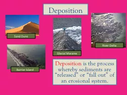
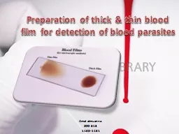
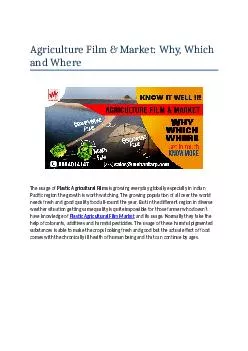
31 Page Physical Chemical 1 Resistive Heating 2 Flash Evaporation 3 Electron Beam Evaporation 4 Laser Evaporation 5 Arc Evaporation 1 Glow Discharge Sputtering 2 Triode Sputtering 3. California Deposition Reporters takes pride in our reporters by providing you with experienced reporters who arrive early to court and depositions, and provide the kind of service dictated in the professional atmosphere in which they take the spoken word and put into print witness' testimony utilizing the many tools utilized in today's market. They are then able to provide to you in many formats the transcripts either electronically or on paper. With scanned, linked and searchable exhibits. California Deposition Reporters takes pride in our reporters by providing you with experienced reporters who arrive early to court and depositions, and provide the kind of service dictated in the professional atmosphere in which they take the spoken word and put into print witness' testimony utilizing the many tools utilized in today's market. They are then able to provide to you in many formats the transcripts either electronically or on paper. With scanned, linked and searchable exhibits. (PVD and CVD). 1. Plan of presentation. Deposition methods. . CVD(. . Chemical . Vapor . Deposition) . . PVD ( Physical . Vapor . Deposition. ). Principles, processes on . the surface . . 2. by . means of MBE method. Ashida. . lab. M1 . K. amizono Kenta. Introduction. All-optical switching devices. Excitons . and light in the high-quality system . Background . Previous results. Temperature dependence of DFWM spectrum. Physical Weathering. Weathering. is the breakdown of rock or soil. . Physical . weathering occurs when natural forces, such as wind, running water, and moving ice, physically break up rock and soil into smaller particles. . Deposition. is the process whereby sediments. are “released” or “fall out” of an . erosional system.. River Delta. Glacial Moraine. Sand Dune. Barrier Island. Factors. that Impact . Deposition -- Velocity. 1. Fact Pattern. In . the early hours of March 28, 2011, . Wayne “Crash” Wayward. was operating a tour bus for a transportation company called . Gospel Escort Services. when the bus caught fire. Wayward was transporting a renowned gospel music band called . Part III: Summarizing Depositions. PART I: Last Minute Depo Tips!. GAP: Week 6 The Deposition. Professor Roxanne Crocket ’03 – Graves & King. Professor Donald G. Forgey ‘77 – Lewis Brisbois . pH Scale. PRIMARY POLLUTANTS (sulfur dioxide & nitrogen oxides) are emitted by combustion.. Primary pollutants can travel as far as 1,000 km. .. As the primary pollutants react with H. 2. O vapor and O. Impact on Ecosystems. . The study of environmental chemistry involves more than just the . detection of . substances. . Scientists . who study the environment conduct . investigations to . determine whether there is evidence of change in the environment.. Amal. . almuanna. ZOO 515 . 1433-1434. Materials. Glass slide. Coverslips. alcohol swabs . Gloves . Microscope. pencil. . Capillary blood obtained by . fingerstick. : . 1. Label pre-cleaned slides (preferably frosted-end) with patient’s name (or other identifier), date and time of . in ASTeC. Oleg Malyshev and Reza Valizadeh. 1. The aim of TF SRF programme. SRF programme at ASTeC started six years ago from no infrastructure and it aims from beginning was to stablish know how for depositing SRF thin film in RF (. The usage of plastic agricultural films is growing every day globally especially in India in the agricultural tarpaulin films market. Four types of agricultural films like - geomembrane films, silage films & sheets, mulch films, and greenhouse films. Matthew Burton. The College of William & Mary. Department of Physics. Acknowledgements. Research Group:. Melissa Beebe (W&M), Ari . Palczewski. (JLab),. Larry Phillips (JLab), Charlie Reece (JLab) and Ale Lukaszew (W&M).
Download Rules Of Document
"Thin Film Deposition Technique"The content belongs to its owner. You may download and print it for personal use, without modification, and keep all copyright notices. By downloading, you agree to these terms.
Related Documents