/
Production of precise large PCB’s Production of precise large PCB’s

Production of precise large PCB’s - PowerPoint Presentation

luanne-stotts
luanne-stotts . @luanne-stotts
Follow
378 views
Uploaded On 2016-06-21

Production of precise large PCB’s - PPT Presentation

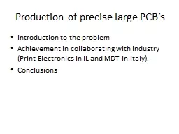
Introduction to the problem Achievement in collaborating with industry Print Electronics in IL and MDT in Italy Conclusions Introduction to the problem Need to construct large PCB with precise strips over surfaces of 21X12m² flat to within 50 ID: 371234

precision boards layer large boards precision large layer pcb print thickness strips alignment machining industry introduction precise

Share:

Link:

Embed:

Download Presentation from below link

Download Presentation The PPT/PDF document "Production of precise large PCB’s" is the property of its rightful owner. Permission is granted to download and print the materials on this web site for personal, non-commercial use only, and to display it on your personal computer provided you do not modify the materials and that you retain all copyright notices contained in the materials. By downloading content from our website, you accept the terms of this agreement.


Presentation Transcript

Slide1

Production of precise large PCB’s

Introduction to the problem

Achievement in collaborating with industry (Print Electronics in IL and MDT in Italy).

Conclusions Slide2

Introduction to the problem

Need to construct large PCB with precise strips over surfaces of 2.1X1.2m², flat to within 50

μ

m that can be aligned with respect to each other within the same precision.Slide3

Introduction

Single PCB’s can be purchased with dimensions of 1.28X3.00m² that are flat to within 50

μ

m, except at the edges.Using usual PCB print methods are not very reproducible to the precision one needs.

One needs VERY PRECISE external references, in order to align each plane with the design accuracy.CNC machining provides the necessary accuracy.Combined the 2 technologies. Slide4

Method utilize to get the precision

Use the inserts that are machined together with the strips to get the precisionSlide5

Use a precision jig to transfer the precision across layersSlide6

Achieved results (MDT)

Introduce brass inserts that are machined together with the strips and then use PCB multilayer techniques to apply the 100

μ

m isolating layer, on which the graphite can be applied.Slide7

The pads boards are 4 layer boards

Only precision on the thickness is needed.

Outside ground layer provides the needed impedance matching.Slide8

Pad boardsSlide9

Thickness uniformity of large boards

All boards are within the 50

μ

m rms

The worst one (50μm rms) is due to a defect of fabrication (wrong machining of connection lines that were re-made for the pads) Slide10

Performing the measurement of position of

plane1-plane2 (remember offset is 1.45mm)

At 2 different positions, spaced by 45cm, gives a difference of

2

0+/-36μm, consistent with good alignment but limited by the statistics. Boards fabricated by Print Electronics in Israel

Mean = -1420 ± 25 µm

Mean = -1440 ± 26 µm

Relative alignment between 2 planes using this method were measured in smaller (40X60cm²) detectorsSlide11

Conclusions

Industry is able to achieve the necessary requirements on relative alignment between layers (50

μ

m over 1m) for large boards, by combining mechanical machining with multi-layer PCB techniques.By eliminating the edges of the boards, a thickness uniformity of better than 50μ

m over large surfaces has been achieved by industry.