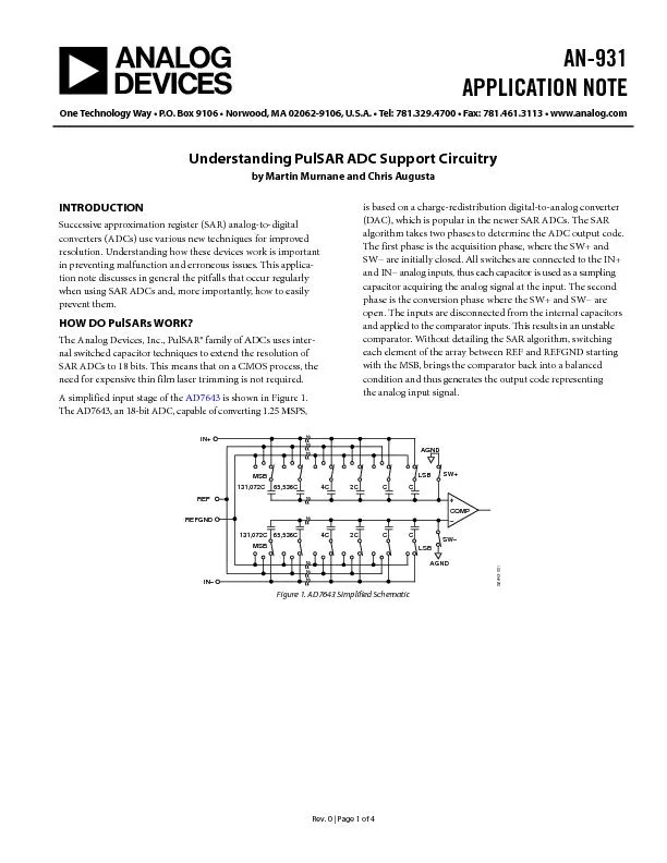
/
APPLICATION NOTEONE TECHNOLOGY WAY  P.O. BOX 9106 APPLICATION NOTEONE TECHNOLOGY WAY  P.O. BOX 9106

APPLICATION NOTEONE TECHNOLOGY WAY P.O. BOX 9106 - PDF document

marina-yarberry
marina-yarberry . @marina-yarberry
Follow
387 views
Uploaded On 2016-03-19

APPLICATION NOTEONE TECHNOLOGY WAY P.O. BOX 9106 - PPT Presentation

a 7813294700 those listed above HVPS t Figure 1Human Body Model I t 200pF Figure 2Machine Model 1 DIELECTRICGROUND PLANE DISCHARGECHARGE t Figure 3Charged Device Modelwards 0V with a fall ti ID: 262441

a 781/329-4700 those listed above. HVPS t Figure 1.Human

Share:

Link:

Embed:

Download Presentation from below link

Download Pdf The PPT/PDF document "APPLICATION NOTEONE TECHNOLOGY WAY P.O...." is the property of its rightful owner. Permission is granted to download and print the materials on this web site for personal, non-commercial use only, and to display it on your personal computer provided you do not modify the materials and that you retain all copyright notices contained in the materials. By downloading content from our website, you accept the terms of this agreement.


Presentation Transcript

a APPLICATION NOTEONE TECHNOLOGY WAY P.O. BOX 9106 781/329-4700 those listed above. HVPS t Figure 1.Human Body Model I t 200pF Figure 2.Machine Model 1 DIELECTRICGROUND PLANE DISCHARGECHARGE t Figure 3.Charged Device Modelwards 0V� with a fall time of 150ns. MIL-STD-883 requires a rise time of ns and a delay time of 20ns (Method 3015 defines delay time as the time or 0.267A. Althoughthis peak current is much lower than that for 400V CDM t 642–420ns/DIVt 14ns, i.e., only slightly greater than that of theever, the peak current for the first peak of the 400V MM which is the highest of the three models. RLC7,500nH,100pF.(typically7,500nHRLCɏɏ500nH,200pF. RLC~25ɏ(sparkresistance),pF. …3…Table I. ModelHBMMMSocketed CDM MachineCharged DeviceOriginUS MilitaryJapan 1976AT&T 1974 Late 1960s Real WorldYesGenerally NoYes RC1.5k, 100pF0 , 200 pF1 Rise Timens14 ns* at 400V0.27 A5.8 A*2.1 A** DependentNoNoYes RecoveryNoNoYes *These values are per ESD Association Standard S5.2. EIAJs stan-**These values are for the direct charging (socketed) method.When auditing a facility in which ESD protective mea-a)Personal ground strap (wrist strap)b)Conductive trays or shunts, etc.c)Conductive work surfaced)Conductive floor or mate)A common ground pointable range is 40 to 60 percent. Where high relative Training: Keep in mind, the key to an effective ESDcontrol program is TRAINING.Ž Training should beten best left to Failure Analysis Engineers.Typicallyperformed.In the case of ESD, events of 1kV or morejunctions in less than 10 ns (see Figure 6).Alternately,1ms can cause sufficient self-heating of Figure 5.Scanning Electron Microscope View of a Figure 6.Scanning Electron Microscope Cross-Sectional View of a CDM ESD Site.This subsurface site JS-001-2011 JESD22-C101E JESD22-A115B Test Method) chargingCDMchargehavepeakcurrentbetweenpackagetheresultsdischargeSummarycomparescharacteristicsthethree Standard Document subjected to an ESD event.In order to perform this OPEN CIRCUIT V/DIV. : 2V I/DIV. : 50 GOOD TRACE Figure 7.Example of an Unpowered Curve Traceand negative supplies together.If current flow is notlimited, electrical overstress will occur.The classic case SCR structureevent. The SCR turns on and essentially causes a short and ground.of the parasitic transistors is turned on. The current re-transistor.In turn, the collector current of the secondtransistor maintains a forward bias on the base-emitterof the first transistor.If the product of the two transistor OUTPUTV Figure 8.Parasitic SCR.The Diffusions in a CMOSoutput form a parasitic SCR.The resistors are labeledFigure 9a.Output Overvoltage Triggering.Initial holeFigure 9b.Current Multiplication.The substrateage drop to sustain the latch-up condition. A value of triggering mechanism occurs if a supplyrail.Unlike the case of I/O triggering, latch-up can occurunder the Absolute Maximum Rating specification.Ifoccur. Operating a device near the maximum ratingsmay degrade the long term reliability of the device. Also p+ n+ n+ p+ p+ n+ GNDOUTPUT OUTPUTGNDV +V n+ n+ p+ GNDOUTPUT + INPUT 1.Digital inputs and outputs should not be allowed to by more than 0.3 volts at any time. This = 0 volts.2.Digital inputs and outputs should also not be allowed3.For mixed signal devices, DGND should not be al-4.For a CMOS or Bipolar-CMOS DAC, I should, inthan 0.3 volts.Some DACs can tolerate significant current flow, however, without any danger of1.If the digital inputs or outputs of a device can go be- at any time, a diode (such as a 1N914) con- will prevent SCR action andsubsequent latch-up.This works because the diode pin, thus prevent-ing SCR triggering.This is shown in Figure 10. supply rail (the IbIc IC POWERED UPIC#1OUT0VIC POWERED DOWN DGNDCOMMON GROUNDOUTPUT Figure 10.Adding an inexpensive silicon diode in to this rule is when thesions at …0.3 volts to …0.4 volts. This prevents thetriggering.Figure 11 shows the connections for the R OUT DGNDCOMMON GROUNDV 2835RINDUCTANCE 2835 INPUT CLAMPEDAND DAMPED Figure 11.Adding Schottky diodes from the inputsNPN, thus inhibiting SCR action.The series damp-3.If the DGND potential can occasionally exceed AGNDshown in Figure 12.An extra diode connected in in-cation for each pin. Set the Time/Div. to the minimum4. In circuits where the I pin of a CMOS IC can be …6… PNPVERTICALNPN R1R2R4 DGNDAGNDFigure 12.Connecting Schottky diodes betweenICs from latching up. This condition sometimes oc-ing a DAC. During power-up or power-down transi- to the negative supply rail. An5.In designs that have long digital PC board traces be- will be beneficial.This resistor increasesTransZorb* transient voltage suppressor (TVS). What is (TVSs) are devices usedtransient appears.Electrical parameters such as break- caused by the temperature coefficient of the TVS, Industries, Inc. Figure 13.Transients of several thousand volts can bespecified for voltage regulation.Therefore, for transientThe surge power and surge current capability of theTVS are proportional to its junction area. Surge ratingsfor silicon TVS families are normally specified in kilo-s test waveform. Power ratings range froms.Thisments from 5 V up to 376 V for some families. Because and a duration of 10/1000the TVS must clamp at 40 V or less.The current deliv- = 50Asource impedance and the TVS device.Thus the TVS …7…TYPICAL TVS APPLICATIONSDC Line ApplicationsTransZorb TVSs on power lines prevent IC failurescaused by transients, power supply reversals or duringswitching of the power supply between on and off(Figure 16). Ic Figure 16.For power sources utilizing the TransZorb TVS, theTransZorb TVS is chosen such that the reverse stand-offvoltage is equal to or greater than the dc output voltage.For certain applications it may be more desirable to re-place the series resistor (R) with an inductor (Figure 17). RECTIFIERNETWORKRDC wires.Limited protection is provided by the clamp Ic OR 10,000 volts in magnitude.Excess current passing SIGNAL WIRE age leaving a net source voltage of 100V.When theThis circuit can be protected with a 5kW rated TransZorb TRANSIENTLOAD Figure 14.A 5 kW TVS is required to handle the surge15.Since the current drawn by the transducer undernormal operation is small (mA typical), perfor-For a small load current, 10mA, the voltage drop acrossthe added resistance is minimal, about 250mV for a25ohm resistor. Adding this resistor reduces the surgeI = (140V … 40V)/(2) = 3.7Aresistor.A TVS with lower power rating is able tohandle the resulting current.In this case a 500W sup-pressor replaces the 5kW device, saving board space 28V Figure 15.The series resistor reduces transient currentity. Steady state power dissipated by the resistor (V2.5mW requiring the lowest rated resistor available for solution that depends on many factors. The following is1.Personnel should be trained in the proper handling2.A good facilities ground system including shielding3.Use transient suppressors judiciously, i.e., check if4.Review the proper power-up sequence of the and finally all other pins.5.Review the data sheet, in particular the maximum rat-if latent damage may be present.This analysis shouldDevices publications; (1) Joe Buxton, ŽSimple Tech- 28-3, 1994, and (2) Joe Buxton, ŽInputLatch-Up in CMOS DACs, AN-109. Free from Analog, pp. 633, 696…703. Contains ad- ©1995…2012 Analog Devices, Inc. All rights reserved. Trademarks and registered trademarks are the property of their respective owners. AN10536-0-2/12(A)