/
ApplicationReport ApplicationReport

ApplicationReport - PDF document

min-jolicoeur
min-jolicoeur . @min-jolicoeur
Follow
551 views
Uploaded On 2015-08-18

ApplicationReport - PPT Presentation

SLVA317B ID: 109773

SLVA317B

Share:

Link:

Embed:

Download Presentation from below link

Download Pdf The PPT/PDF document "ApplicationReport" is the property of its rightful owner. Permission is granted to download and print the materials on this web site for personal, non-commercial use only, and to display it on your personal computer provided you do not modify the materials and that you retain all copyright notices contained in the materials. By downloading content from our website, you accept the terms of this agreement.


Presentation Transcript

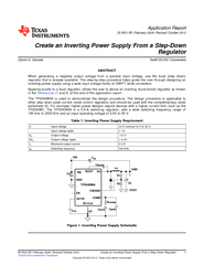
ApplicationReport SLVA317B–February2009–RevisedOctober2012 CreateanInvertingPowerSupplyFromaStep-Down Regulator DavidG.Daniels..............................................................................................SwiftDC/DCConverters ABSTRACT Whengeneratinganegativeoutputvoltagefromapositiveinputvoltage,usethebuck(stepdown) regulatorthatisalreadyavailable.Thisstep-by-stepprocedurehelpsguidetheuserthroughdesigningan invertingpowersupplyusingawideinputvoltagefamilyofSWIFTdc/dcconverters. Applyingdualitytoabuckregulator,allowstheusertoderiveaninverting(buck-boost)regulatorasshown intheReferences(1and2)attheendofthisapplicationreport. TheTPS54060Aisusedtodemonstratethedesignprocedure.Thedesignprocedureisapplicableto otherstepdownpeakcurrentmodecontrolregulatorsandshouldbeusedwiththecomplementaryexcel worksheet(5).Forexample,higherpowerdesignsrequiredeviceswithahighercurrentlimit,suchasthe TPS54360.TheTPS54060Aisa0.5-Aswitchingregulator,withawideswitchingfrequencyrangeof 100kHzto2500kHzandaninputoperatingvoltageof3.5Vto60V. Table1.InvertingPowerSupplyRequirement VI Inputvoltage 24Vnominal18Vto30V Inputvoltageripple 1% VO Outputvoltage –12V dVO Outputvoltageripple 0.5% IO Maximumoutputcurrent 0.3A fsw Switchingfrequency 500kHz Figure1.InvertingPowerSupplySchematic 1 SLVA317B–February2009–RevisedOctober2012 CreateanInvertingPowerSupplyFromaStep-DownRegulator SubmitDocumentationFeedback Copyright©2009–2012,TexasInstrumentsIncorporated www.ti.com OutputVoltage Thedifferenceinthemaximuminputvoltage,VImax,andtheoutputvoltage,VOshouldnotexceedthe maximumoperatingdevicevoltageoftheregulator.FortheTPS54060A,themaximumoperatingdevice voltage,Vdevmax,is60V. (1) (2) AssumingVOis–12VandusingEquation1,themaximuminputvoltageforthepowersupplycouldbeas highas48V,easilysupportingthe30-VmaximuminputrequirementinTable1.UseEquation2to determineR1fortheoutputdesiredvoltage,setR2equalto1kŸandVrefto0.8VfortheTPS54060A.R1 equals14kŸ. InputVoltageRange Theoperatinginputvoltage,VIminofthepowersupplyshouldbegreaterthantheminimumdevice voltage,Vdevmin.FortheTPS54060A,theVdevminis3.5VTheminimuminputvoltagerequirementforthe powersupplyis18V,thus,satisfyingEquation3. (3) DutyCycle TheidealdutycyclefortheinvertingpowersupplyisshowninEquation4,neglectingthelossesofthe powerswitching,inductoranddiodedrop.Theoutputvoltage,VO,isnegativeandtheinputvoltage,VI,is positiveyieldingapositiveresultforEquation4. (4) Themaximumdutycycle,Dmax,iscalculatedbyusingtheminimuminputvoltage,VIminissubstitutedfor inputvoltage,VIinEquation4.Assuming18VforVIandaVOof–12V,themaximumdutycycle,Dmax, is0.40. OutputCurrent Toestimatewhethertheselectedswitchingregulatorwillbecapableofdeliveringtheoutputcurrent,use Equation5.Theusermustknowthedevice’sminimumcurrentlimit,ICLmin,maximumdutycycle,Dmax, andestimatetheinductorripplecurrentvalue,ILripple. (5) Assumingtheminimumcurrentlimitis0.6AandtheILrippleis25%oftheminimumcurrentlimit,the maximumoutputcurrentthatissupportedbytheTPS54060Aisestimatedtobe315mA. Sincetheinputvoltagerangeandmaximumoutputcurrentissupportedbytheselectedregulator,thenext stepsaretocalculatetheinductorvalue,switchingfrequencyandoutputcapacitorvalue. Themaximumswitchingfrequencyshouldbecalculatedusingtheminimumcontrollableontime, maximuminputvoltageandsomeofthelossesinthesupply.Ifthemaximumfrequencycalculatedis greaterthanthe2500kHzsupportedbytheTPS54060A,limittheƒskipmaxto2500kHz. (6) AconsiderationspecificallyfortheTPS54060Adeviceisthefrequencyshiftthatoccurstoprevent overcurrentrunawayduringanoutputshortcircuit (7) 2 CreateanInvertingPowerSupplyFromaStep-DownRegulator SLVA317B–February2009–RevisedOctober2012 SubmitDocumentationFeedback Copyright©2009–2012,TexasInstrumentsIncorporated www.ti.com Themaximumswitchingfrequencywillbethelowerfrequencyofƒshiftmaxorƒskipmax.TheVOsctermin Equation7istheoutputvoltageduringtheoutputfault.Theƒdivisthefrequencydivision.ƒdivis8when VOscislessthan25%oftheregulationvoltage.SeetheSelectingtheSwitchingFrequencysectionof TPS54060Adatasheetformoredetailsonthefrequencyshift.Theminimumontime,tOmin,is130nsand themaximumMOSFETonresistance,Rhs,is400mŸfortheTPS54060A.Assumingdiodevoltagedrop, Vfd,is0.5V,inductorresistance,Rdc,is325mŸ,themaximumfrequencycalculatedis2286kHzand 1210kHz,usingEquation6andEquation7,respectively.Themaximumswitchingfrequencyselected shouldnotbegreaterthan1210kHz.Sincethepowersupplyspecificationrequirementfortheswitching frequencyis500kHzandislowerthanthe1210kHz,nodesignchangesarenecessary. Inductor Todeterminetheinductorvalue,calculatetheaverageinductorcurrent,ILavg,atthemaximumoutput currentandmaximuminputvoltage. UsethemaximuminputvoltageasavariableinEquation4tocalculateminimumdutycycle,Dmin. AssumingVImaxis30V,Dminisapproximately0.286andILavgis0.42A. Theinductorvalueiscalculated,Equation9,usingaripplecurrentthatis25%oftheaverageinductor current.UsingtheDmintocalculatetheminimuminductancevaluegivesthelargestinductance. AssumingVImaxof30V,IOof0.3Aandaƒswof500kHz,theLoiscalculatedas163H.Thenearest standardinductorof150Hisusedfortheinductor.Theinductorsaturationcurrentshouldbegreater thanthe0.548AofpeakcurrentcalculatedinEquation10.Theinductorrmscurrentshouldbegreater than0.450AcalculatedinEquation11. (8) (9) (10) (11) OutputCapacitor Theoutputcapacitormustsupplythecurrentwhenthehighsideswitchison.Usetheminimuminput voltagetocalculatetheoutputcapacitanceneeded.Thisiswhenthedutycycleandthepeak-to-peak currentintheoutputcapacitoristhemaximum.Usingthe0.5%voltageripplespecification,dVO,and Equation12,COminis4F.Assumingthe0.5%voltagerippleandmaximumdutycycle,theRc, equivalentseriesresistanceshouldbelessthan109mŸ,usingEquation13.Thermscurrentforthe outputcapacitoris0.245AusingEquation14.Two15F/25VX5Rinparallelareusedfortheoutput capacitorbecauseofthelowESRandsize. (12) (13) (14) DiodeSelection Thediodevoltageneedstobegreaterthanthedifferenceofthemaximuminputvoltageandoutput voltage.Fortheexampledesign,thediodeneedstosupportavoltagegreaterthan42V. 3 SLVA317B–February2009–RevisedOctober2012 CreateanInvertingPowerSupplyFromaStep-DownRegulator SubmitDocumentationFeedback Copyright©2009–2012,TexasInstrumentsIncorporated www.ti.com UsingEquation15,thepowerdissipationiscalculatedusingthediodeforwardvoltagedrop,Vƒd,atthe maximuminputvoltageandtheaveragediodecurrent.AssumingVƒdof0.5V,Pdiodeis0.150W.The peakcurrentinthediodeisthesameastheinductor,Equation10.Selectadiodewhichhasapower ratinggreaterthan0.107Wandsupportstheinductorcurrent. (15) PowerDissipationinPackage Thepowerdissipationinthepackageisdominatedbytheconductionlossesandswitchinglossesofthe powerswitchandshouldnotexceedthelimitationsofthepackage.Theconductionandswitchinglosses arecalculatedusingEquation16.Theconductionlossesareafunctionofthedutycycle,D,inductorrms current,ILrms,andonresistance,Rhs.Theswitchinglossesareafunctionoftheturnon,tr,andturnoff,tf, times,switchingfrequency,outputcurrent,inputandoutputvoltage. (16) ILrmsiscalculatedtobe0.45Aatnominaldutycycle.Pdeviceis0.2295Wassumingatrandtfof25ns. FrequencyResponseoftheInvertingRegulator Usingabuckregulatortogenerateanegativeoutputdoesnotclosethefeedbackloopaswouldabuck powersupply.So,adifferentdesignmethodisneeded.Theinvertingpowersupplytransferfunctionhas twozeroesandapole.Equation17isasimplifiedtransferfunctionofaninvertingpowersupply,see AppendixAinReferences(3)ortheapplicationreport(4)formoredetailsonthederivation.TheESR zero,ƒz1,isthesameasinaBuckregulator,Equation18,andisafunctionoftheoutputcapacitorandits ESR.Theotherzeroisarighthalfplanezero,ƒz2.Thefrequencyresponseoftheƒz2resultsinan increasinggainandadecreasingphase.Theƒz2frequencyisafunctionofthedutycycle,outputcurrent, andtheinductor.Equation19calculatestheminimumfrequencyoftheƒz2whichisusedtodeterminethe crossoverfrequency.Thedominantpole,ƒp1,isafunctionoftheloadcurrent,outputcapacitorandduty cycle,seeEquation20.Kbbisthedcgainandisusedtocalculatethefrequencycompensation components.Thegmpsvariableisthetransconductanceofthepowerstage,whichis1.9A/Vforthe TPS54060A. Theƒz1isestimatedtobe1516kHz.Theoutputcapacitorisderatedby30%becauseofthedcvoltage andtheESRisassumedtobe5mŸ.Theƒz2isestimatedtobe38.3kHz.Assumingresistanceofthe inductor,Rdcis325mŸ.Theƒp1isestimatedtobe253Hzassuminganominaldutycycle.Kbbis calculatedas38V/Vassumingnominalinputvoltage. (17) (18) (19) (20) (21) 4 CreateanInvertingPowerSupplyFromaStep-DownRegulator SLVA317B–February2009–RevisedOctober2012 SubmitDocumentationFeedback Copyright©2009–2012,TexasInstrumentsIncorporated www.ti.com Thecrossoverofthepowersupplyshouldbesetbetweentheƒp1and1/3ofƒz2frequencies.Itis recommendedtostartwiththecrossoverfrequency,ƒco,givenbyEquation22.Theƒcoisestimatedto be3.1kHz. (22) Thecompensationresistor,Rcomp,neededtosetthecompensationgainatthefcofrequencyiscalculated usingEquation23.TheVrefis0.8Vandgmeais92A/VfortheTPS54060A. (23) SubstituteƒcointoEquation23,tocalculateRcomp.Rcompisequalto52.8kŸ.Usetheneareststandard valueof52.3kŸ.Thecompensationzeroissetto½ofthedominantpole,ƒp1.Tocalculatethe compensationzerocapacitor,Czero,useEquation24.Equation24gives24nF,usethenextlarger standardvaluewhichis27nF.ThecompensationpoleissettoequaltheRHPzero,ƒz2.Use Equation25,tocalculatethefrequencycompensationpole,Cpolewhichgives79pF.Thenextstandard valueis82pF. (24) (25) InputCapacitors TheTPS54060Aneedsatightlycoupledceramicbypasscapacitor,CdinFigure1,connectedtotheVIN andGNDpinsofthedevice.SincethedeviceGNDisthepowersupplyoutputvoltage,thevoltagerating ofthecapacitormustbegreaterthanthedifferenceinthemaximuminputandoutputvoltageofthepower supply.Itisrecommendedtousea1F/X5R/50V. Equation26toEquation29areusedtoestimatethecapacitance,maximumESR,andcurrentratingfor theinputcapacitor,CI. (26) (27) (28) (29) SlowStartTime PlacingasmallceramiccapacitorontheSS/TRtothechipGND(thatis,systemVO)adjuststheslowstart timeontheTPS54060A.TheslowstartcapacitoriscalculatedusingEquation30.Theequationassumes a2Apullupand10%to90%measurementfortime. (30) 5 SLVA317B–February2009–RevisedOctober2012 CreateanInvertingPowerSupplyFromaStep-DownRegulator SubmitDocumentationFeedback Copyright©2009–2012,TexasInstrumentsIncorporated www.ti.com FrequencySetResistor Theswitchingfrequencyissetwitharesistor,RT,fromtheRT/CLKpintotheGNDoftheTPS54060A device.UseEquation31toestimatethefrequencysetresistor. (31) SynchronizingtoanExternalClock TheTPS54060AhasaCLKpinthatcanbeusedtosynchronizethepowersupplyswitchingfrequencyto anexternalsystemclock.Butalevelshiftcircuitneedstobeusedtotranslateasystemgroundreference clocksignaltothedevice’sground. StartVoltage Whenusedasastepdownregulator,theTPS54060Ahasanadjustablestartandstopvoltagesetby usingresistorsontheENpin.Thestopvoltageislowerthanthestartvoltage.Whenusedasaninverting powersupplyonlythestartvoltagecanbeuseful.Aftertheinvertingpowersupplystartsup,theeffective inputvoltagetheTPS54060Adeviceexperiencesrisesastheoutputvoltagereachesfullregulation. Therefore,itisrecommendedtousealowervalueresistoronthehighsidetominimizethehysteresis voltage.Theinputvoltagemustdropbytheoutputvoltageandthehysteresisvoltagetoshutdownthe supply.SeetheEnableandAdjustingUndervoltageLockoutsectionoftheTPS54060Adatasheetforthe equation. Figure2.24Vto–12V/0.3APowerSupply ExperimentalResults Figure3toFigure16showtheexperimentaltestresultsoftheFigure2design.Thediscontinuous conductionmode(DCM)tocontinuousconductionmode(CCM)boundaryisatanoutputcurrentof27 mA.Thepulseskipmode(PSM)boundaryisatanoutputcurrentof2.5mA.Theinputcurrentdrawatno loadat24Vinputvoltageis1.77mA. 6 CreateanInvertingPowerSupplyFromaStep-DownRegulator SLVA317B–February2009–RevisedOctober2012 SubmitDocumentationFeedback Copyright©2009–2012,TexasInstrumentsIncorporated www.ti.com Figure3.EfficiencyVersusLoadCurrent Figure4.LightLoadEfficiencyVersusLoadCurrent Figure5.OutputVoltageVersusLoadCurrent Figure6.OutputVoltageVersusInputVoltage Figure7.OutputVoltageRippleat0.3A Figure8.OutputVoltageRippleatDCM 7 SLVA317B–February2009–RevisedOctober2012 CreateanInvertingPowerSupplyFromaStep-DownRegulator SubmitDocumentationFeedback Copyright©2009–2012,TexasInstrumentsIncorporated www.ti.com Figure9.OutputVoltageRippleatPSM Figure10.InputRippleCCMATIO=0.3A Figure11.InputRippleDCM Figure12.InputRipplePSM Figure13.VOStartupwithVI Figure14.StartUpwithENandInput 8 CreateanInvertingPowerSupplyFromaStep-DownRegulator SLVA317B–February2009–RevisedOctober2012 SubmitDocumentationFeedback Copyright©2009–2012,TexasInstrumentsIncorporated www.ti.com Figure15.LoadTransient Figure16.OverallLoopFrequencyResponse References 1.Usingabuckconverterinaninvertingbuck-boosttopology,JohnTucker,LiteratureNumberSLYT286, 4Q2007AnalogApplicationsJournal,TexasInstruments. 2.UsingtheTPS5430asanInvertingBuck-BoostConverter,JohnTucker,LiteraturenumberSLVA257A, ApplicationReport,August20078,TexasInstruments. 3.AchievingHigh-EfficiencywithaMulti-OutputCCMFlybackSupplyUsingSelf-DrivenSynchronous Rectifiers,RobertKollman,LiteratureNumberSLUP204,SEM1500SeminarPaper,Texas Instruments. 4.UnderstandingBuck-BoostPowerStagesinSwitchModePowerSupplies,EverettRogers,Literature NumberSLVA059A-March1999ApplicationReport,TexasInstruments. 5.“TPS54060AINVERTING.xls”excelworksheet(SLVC211A),2009TexasInstrumentsIncorporated. www.ti.com. 9 SLVA317B–February2009–RevisedOctober2012 CreateanInvertingPowerSupplyFromaStep-DownRegulator SubmitDocumentationFeedback Copyright©2009–2012,TexasInstrumentsIncorporated IMPORTANTNOTICE TexasInstrumentsIncorporatedanditssubsidiaries(TI)reservetherighttomakecorrections,enhancements,improvementsandother changestoitssemiconductorproductsandservicesperJESD46,latestissue,andtodiscontinueanyproductorserviceperJESD48,latest issue.Buyersshouldobtainthelatestrelevantinformationbeforeplacingordersandshouldverifythatsuchinformationiscurrentand complete.Allsemiconductorproducts(alsoreferredtohereinas“components”)aresoldsubjecttoTI’stermsandconditionsofsale suppliedatthetimeoforderacknowledgment. TIwarrantsperformanceofitscomponentstothespecificationsapplicableatthetimeofsale,inaccordancewiththewarrantyinTI’sterms andconditionsofsaleofsemiconductorproducts.TestingandotherqualitycontroltechniquesareusedtotheextentTIdeemsnecessary tosupportthiswarranty.Exceptwheremandatedbyapplicablelaw,testingofallparametersofeachcomponentisnotnecessarily performed. TIassumesnoliabilityforapplicationsassistanceorthedesignofBuyers’products.Buyersareresponsiblefortheirproductsand applicationsusingTIcomponents.TominimizetherisksassociatedwithBuyers’productsandapplications,Buyersshouldprovide adequatedesignandoperatingsafeguards. TIdoesnotwarrantorrepresentthatanylicense,eitherexpressorimplied,isgrantedunderanypatentright,copyright,maskworkright,or otherintellectualpropertyrightrelatingtoanycombination,machine,orprocessinwhichTIcomponentsorservicesareused.Information publishedbyTIregardingthird-partyproductsorservicesdoesnotconstitutealicensetousesuchproductsorservicesorawarrantyor endorsementthereof.Useofsuchinformationmayrequirealicensefromathirdpartyunderthepatentsorotherintellectualpropertyofthe thirdparty,oralicensefromTIunderthepatentsorotherintellectualpropertyofTI. ReproductionofsignificantportionsofTIinformationinTIdatabooksordatasheetsispermissibleonlyifreproductioniswithoutalteration andisaccompaniedbyallassociatedwarranties,conditions,limitations,andnotices.TIisnotresponsibleorliableforsuchaltered documentation.Informationofthirdpartiesmaybesubjecttoadditionalrestrictions. ResaleofTIcomponentsorserviceswithstatementsdifferentfromorbeyondtheparametersstatedbyTIforthatcomponentorservice voidsallexpressandanyimpliedwarrantiesfortheassociatedTIcomponentorserviceandisanunfairanddeceptivebusinesspractice. TIisnotresponsibleorliableforanysuchstatements. Buyeracknowledgesandagreesthatitissolelyresponsibleforcompliancewithalllegal,regulatoryandsafety-relatedrequirements concerningitsproducts,andanyuseofTIcomponentsinitsapplications,notwithstandinganyapplications-relatedinformationorsupport thatmaybeprovidedbyTI.Buyerrepresentsandagreesthatithasallthenecessaryexpertisetocreateandimplementsafeguardswhich anticipatedangerousconsequencesoffailures,monitorfailuresandtheirconsequences,lessenthelikelihoodoffailuresthatmightcause harmandtakeappropriateremedialactions.BuyerwillfullyindemnifyTIanditsrepresentativesagainstanydamagesarisingoutoftheuse ofanyTIcomponentsinsafety-criticalapplications. Insomecases,TIcomponentsmaybepromotedspecificallytofacilitatesafety-relatedapplications.Withsuchcomponents,TI’sgoalisto helpenablecustomerstodesignandcreatetheirownend-productsolutionsthatmeetapplicablefunctionalsafetystandardsand requirements.Nonetheless,suchcomponentsaresubjecttotheseterms. NoTIcomponentsareauthorizedforuseinFDAClassIII(orsimilarlife-criticalmedicalequipment)unlessauthorizedofficersoftheparties haveexecutedaspecialagreementspecificallygoverningsuchuse. OnlythoseTIcomponentswhichTIhasspecificallydesignatedasmilitarygradeor“enhancedplastic”aredesignedandintendedforusein military/aerospaceapplicationsorenvironments.BuyeracknowledgesandagreesthatanymilitaryoraerospaceuseofTIcomponents whichhavenotbeensodesignatedissolelyattheBuyer'srisk,andthatBuyerissolelyresponsibleforcompliancewithalllegaland regulatoryrequirementsinconnectionwithsuchuse. TIhasspecificallydesignatedcertaincomponentswhichmeetISO/TS16949requirements,mainlyforautomotiveuse.Componentswhich havenotbeensodesignatedareneitherdesignednorintendedforautomotiveuse;andTIwillnotberesponsibleforanyfailureofsuch componentstomeetsuchrequirements. Products Applications Audio www.ti.com/audio AutomotiveandTransportation www.ti.com/automotive Amplifiers amplifier.ti.com CommunicationsandTelecom www.ti.com/communications DataConverters dataconverter.ti.com ComputersandPeripherals www.ti.com/computers DLP®Products www.dlp.com ConsumerElectronics www.ti.com/consumer-apps DSP dsp.ti.com EnergyandLighting www.ti.com/energy ClocksandTimers www.ti.com/clocks Industrial www.ti.com/industrial Interface interface.ti.com Medical www.ti.com/medical Logic logic.ti.com Security www.ti.com/security PowerMgmt power.ti.com Space,AvionicsandDefense www.ti.com/space-avionics-defense Microcontrollers microcontroller.ti.com VideoandImaging www.ti.com/video RFID www.ti-rfid.com OMAPApplicationsProcessors www.ti.com/omap TIE2ECommunity e2e.ti.com WirelessConnectivity www.ti.com/wirelessconnectivity MailingAddress:TexasInstruments,PostOfficeBox655303,Dallas,Texas75265 Copyright©2012,TexasInstrumentsIncorporated