/
SNUG San Jose 2002Simulation and Synthesis Techniques forRev 1.2Asynch SNUG San Jose 2002Simulation and Synthesis Techniques forRev 1.2Asynch

SNUG San Jose 2002Simulation and Synthesis Techniques forRev 1.2Asynch - PDF document

min-jolicoeur
min-jolicoeur . @min-jolicoeur
Follow
406 views
Uploaded On 2015-11-07

SNUG San Jose 2002Simulation and Synthesis Techniques forRev 1.2Asynch - PPT Presentation

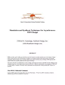
SNUG San Jose 2002Simulation and Synthesis Techniques forRev 12Asynchronous FIFO Designcount value from one clock domain to another is problematic because every bit of annbit counter can change simu ID: 185436

SNUG San Jose 2002Simulation and

Share:

Link:

Embed:

Download Presentation from below link

Download Pdf The PPT/PDF document "SNUG San Jose 2002Simulation and Synthes..." is the property of its rightful owner. Permission is granted to download and print the materials on this web site for personal, non-commercial use only, and to display it on your personal computer provided you do not modify the materials and that you retain all copyright notices contained in the materials. By downloading content from our website, you accept the terms of this agreement.


Presentation Transcript

SNUG San Jose 2002Simulation and Synthesis Techniques forRev 1.2Asynchronous FIFO Design Introductionta values are written to a FIFO buffer from one clockdomain and the data values are read from the same FIFO buffer from another clock domain, where the two clockdomains are asynchronous to each other.Asynchronous FIFOs are used to safely pass data from one clock domain to another clock domain.There are many ways to do asynchronous FIFO design, including many wrong ways. Most incorrectly implementedFIFO designs still function properly 90% of the time. Most almost-correct FIFO designs function properly 99%+ ofthe time. Unfortunately, FIFOs that work properly 99%+ of the time have design flaws that are usually the mostdifficult to detect and debug (if you are lucky enough to notice the bug before shipping the product), or the mostcustomer).This paper discusses one FIFO design style and important details that must be considered when doing asynchronousFIFO design.The rest of the paper simply refers to an “asynchronous FIFO” as just “FIFO.”Passing multiple asynchronous signalsAttempting to synchronize multiple changing signals from one clock domain into a new clock domain and insuringthat all changing signals are synchronized to the same clock cycle in the new clock domain has been shown to beproblematic[1]. FIFOs are used in designs to safely pass multi-bit data words from one clock domain to another.Data words are placed into a FIFO buffer memory array by domain, and the data wordsare removed from another port of the same FIFO buffer memory array by control signals from a second clockdomain. Conceptually, the task of designing a FIFO with these assumptions seems to be easy.The difficulty associated with doing FIFO design is related to generating the FIFO pointers and finding a reliableway to determine full and empty status on the FIFO.For synchronous FIFO design (a FIFO where writes to, and reads from the FIFO buffer are conducted in the sameclock domain), one implementation counts the number of writes to, and reads from the FIFO buffer to increment (onFIFO write but no read), decrement (on FIFO read but no write) or hold (no writes and reads, or simultaneous writepredetermined full value and the FIFO is empty when the FIFO counter is zero.ent-decrement FIFO fill counttwo different and asynchronous clocks would be required to control the counter. To determine full and empty statusnd read pointers will have to be compared.In order to understand FIFO design, one needs to understand how the FIFO pointers work. The write pointer alwayspoints to the next word to be written; therefore, on reset, both pointers are set to zero, which also happens to be thenext FIFO word location to be written. On a FIFO-write operation, the memory location that is pointed to by thewrite pointer is written, and then the write pointer is incremented to point to the next location to be written.Similarly, the read pointer always points to the current FIFO word to be read. Again on reset, both pointers are resetto zero, the FIFO is empty and the readnvalid data (because the FIFO is empty and the empty increments, the empty flag iscleared, and the read pointer that is still addressing the contents of the first FIFO memory word, immediately drivesalways pointing to the next FIFO word to be read mean increment the read pointer SNUG San Jose 2002Simulation and Synthesis Techniques forRev 1.2Asynchronous FIFO Designcount value from one clock domain to another is problematic because every bit of ann-bit counter can change simultaneously (example� 7-8 in binary numbers is� 0111-1000, all bits changed). Oneapproach to the problem is sample and hold periodic binary count values in a holding register and pass aclock domain. When the ready signadomain sends back a synchronized acknowledge signal to the sending clock domain. A sampled pointer must notchange until an acknowledge signal is received from the receiving clock domain. A count-value with multiplerred to a new clock domain using this signal, the sending clock domain has permission to clear the ready signal and re-sample the binary count value.Using this technique, the binary counter values are sampled periodically and not all of the binary counter values canbe passed to a new clock domain The question is, do we need to be concerned about the case where a binary countermight continue to increment and overflow or underflow the FIFO between sampled counter values? The answer isno[8].FIFO full occurs when the write pointer catches up to the synchronized and sampled read pointer. The synchronizedand sampled read pointer might not reflect the current value of the actual read pointer but the write pointer will nottFIFO empty occurs when the read pointer catches up to the synchronized and sampled write pointer. Thesynchronized and sampled write pointer might not reflect the current value of the actual write pointer but the reade readobservations about this technique of sampling binary pointers with a synchronized ready-acknowledge pair ofhandshaking signals are detailed in section 7.0, after the discussion of synchronized Gray[6] code pointers.A common approach to FIFO counter-pointers, is to use Gray code counters. Gray codes only allow one bit tochange for each clock transition, eliminating the problem synchronize multiple changingsignals on the same clock edge.Testing a FIFO design for subtle design problems is nearly impossible to do. The problem is rooted in the fact thatFIFO pointers in an RTL simulation behave ideally, even though, if incorrectly implemented, they can causecatastrophic failures if used in a real design.In an RTL simulation, if binary-count FIFO pointers are included in the design all of the FIFO pointer bits willchange simultaneously; there is no chance to observe synchronization and comparison problems. In a gate-levelsimulation with no backannotated delays, there is only a slight chance of observing a problem if the gate transitionsare different for rising and falling edge signals, and even then, one would have to get lucky and have the correctsequence of bits changing just prior to and just after a rising clock edge. For higher speed designs, the delaydifferences between rising and falling edge signals diminishes and the probability of detecting problems alsodiminishes. Finding actual FIFO design problems is greatest for gate-level designs with backannotated delays, buteven doing this type of simulation, finding problems will be difficult to design problems decreases as signal propagation delays diminish.Clearly the answer is to recognize that there are potential FIFO design problems and to do the design correctly fromThe behavioral model that I sometimes use for testing a FIFO design is a FIFO model that is simple to code, islt to debug if it were used as an RTL synthesis model.This FIFO model is only recommended for use in a FIFO testbench. The model accurately determines when FIFOfull and empty status bits should be set and can be used to determine the data values that should have been stored SNUG San Jose 2002Simulation and Synthesis Techniques forRev 1.2Asynchronous FIFO DesignGray code counter - Style #1Gray codes are named for the person who originally patented the code back in 1953, Frank Gray[6]. There aremultiple ways to design a Gray code counter. This section details a simple and straight forward method to do thedesign. The technique described in this paper uses just one set of flip-flops for the Gray code counter. A secondmethod that uses two sets of flip-flops to achieve higher speeds is detailed in shown in section 4.0.Gray code counter. It would certainly be easy to create the two counters separately, but it is also easy and efficientto create a common n-bit Gray code counter and then modify the 2 MSB to form an (n-1)-bit Gray code counter Figure 2 - n-bit Gray code converted to an (n-1)-bit Gray codeTo better understand the problem of converting an n-bit Gray code to an (n-1)-bit Gray code, consider the exampleof creating a dual 4-bit and 3-bit Gray code counter as shown in Figure 2.The most common Gray code, as shown in Figure 2, is a in any column except theMSB are symmetrical about the sequence mid-point[6]. This means that the second half of the 4-bit Gray code is amirror image of the first half with the MSB inverted.To convert a 4-bit to a 3-bit Gray code, we do not want the LSBs of the second half of the 4-bit sequence to be amirror image of the LSBs of the first half, instead we want the LSBs of the second half to repeat the 4-bit LSB-sequence of the first half.Upon closer examination, it is obvious that inverting the second MSB of the second half of the 4-bit Gray code willproduce the desired 3-bit Gray code sequence in the three LSBs of the 4-bit sequence. The only other problem is because when the sequence changes from 7(Gray 0100) to 8 (~Gray 1000) and again from 15 (~Gray 1100) to 0 (Gray 0000), two bits are changing instead ofjust one bit. A true Gray code only changes one bit between counts. SNUG San Jose 2002Simulation and Synthesis Techniques forRev 1.2Asynchronous FIFO DesignThe first fact to remember about a Gray code is that (only one bit can change from one Gray count to the next). The second fact to remember about a Gray code counteris that most useful Gray code counters must have power-of-2 counts in the sequence. It is possible to make a Graycode counter that counts an even number of sequences but conversions to and from these sequences are generallynot as simple to do as the standard Gray code. Also note that there are no odd-count-length Gray code sequences soone cannot make a 23-deep Gray code. This means that the technique described in this paper is used to make a FIFOthat is 2Figure 3 is a block diagram for a style #1 dual n-bit Gray code counter. The style #1 Gray code counter assumes thatthe outputs of the register bits , either ). The Gray code outputsare then passed to a Gray-to-binary converter (), which is passed to a conditional binary-value incrementer togenerate the next-binary-count-value (), which is passed to a binary-to-Gray converter that generates thenext-Gray-count-value (), which is passed to the register inputs. The top half of the Figure 3 block diagramshows the described logic flow while the bottom half shows logic related to the second Gray code counter asdescribed in the next section. Figure 3 - Dual n-bit Gray code counter block diagram - style #1A dual n-bit Gray code counter is a Gray code counter that generates both an n-bit Gray code sequence (described insection 3.2) and an (n-1)-bit Gray code sequence.The (n-1)-bit Gray code is simply generated by doing an exclusive-or operation on the two MSBs of the n-bit Graycode to generate the MSB for the (n-1)-bit Gray code. This is combined with the (n-2) LSBs of the n-bit Gray codecounter to form the (n-1)-bit Gray code counter[5]. SNUG San Jose 2002Simulation and Synthesis Techniques forRev 1.2Asynchronous FIFO Design Figure 6 - Problems associated with extracting a 3-bit Gray code from a 4-bit Gray codeConsider the example shown in Figure 6 of an 8-deep FIFO. In this example, a 3-bit Gray code pointer is used toaddress memory and an extra bit (the MSB of a 4-bit Gray code) is added to test for full and empty conditions. If theFIFO is allowed to fill the first seven locations (words 0-6) and then if the FIFO is emptied by reading back thesame seven words, both pointers will be equal and will point to address Gray-7 (the FIFO is empty). On the nextwrite operation, the write pointer will increment the 4-bit Gray code pointer (remember, only the 3 LSBs are beingused to address memory), making the MSBs different on the 4-bit pointers but the rest of the write pointer bits willmatch the read pointer bits, so the FIFO full flag would be asserted. This is wrong! Not only is the FIFO full, but the 3 LSBs did not change, which means that the addressed memory location will over-write the last FIFOmemory location that was written. This too is wrong!This is one reason why the dual n-bit Gray code counter of Figure 4 and Section 4.0 is used.The correct method to perform the full comparison is accomplished by synchronizing the into the domain and then there are three conditions that and the synchronized MSB's are not equal (because the must have wrappedone more time than the and the synchronized 2nd MSB's are not equal (because an inverted 2 MSB from one pointer must be tested against the un-inverted 2 MSB from the other pointer, which is required if theMSB's are also inverses of each other - see Figure 6 above). and synchronized bits must be equal.In order to efficiently register the output, the synchronized read pointer is actually compared against the (the next Gray code that will be registered in the ). This is shown below in the sequential alwaysblock that has been extracted from the code of Example 7: SNUG San Jose 2002Simulation and Synthesis Techniques forRev 1.2Asynchronous FIFO Designgn) (wgnext[ADDRSIZE-1] !=wq2_rptr[ADDRSIZE-1]) && (wgnext[ADDRSIZE-2:0]==wq2_rptr[ADDRSIZE-2:0]));always @(posedge wclk or negedge wrst_n) if (!wrst_n) wfull else wfull In the above code, the three necessary conditions to check for FIFO-full are tested and the result is assigned to thewfull_val signal, which is then registered in the subsequent sequential always block.The continuous assignment to can be further simplified using concatenations as shown below:w: wq2_rptr[ADDRSIZE-2:0]});5.3 Different clock speedsSince asynchronous FIFOs are clocked from two different clock domains, obviously the clocks are running atdifferent speeds. When synchra slower clock domain, there will be some count valuesthat are skipped due to the fact that the faster clock will semi-periodically increment twice between slower clockedges. This raises discussion of the two following questions:First question. Noting that a synchronized Gray codeshow multi-bit changes in the synchronized value, will this cause multi-bit synchronization problems?The answer is no. Synchronizing multi-bit changes is only a problem when multiple bits are changing near the risingedge of the synchronizing clock. The fact that a Gray code counter could increment twice (or more) between slowersynchronization clock edges means that the first Gray code change will occur well before the rising edge of therising clock edge. There is no multi-bitsynchronization problem with Gray code counters.rising edge of a slower clock signal, is it possible without recognizing that the FIFO was ever full? Again, the answer is no using the implementation described in this paper. Consider first the generation of FIFO full.The FIFO goes full when the write pointdetected in the write clock domain. If the -domain is faster than the -domain, the write pointer willeventually catch up to the synchronized read pointer, the FIFO will be full, the bit will be set and the FIFOsynchronized read pointer in the -domain.A similar examination of the empty flag shows that the FIFO goes empty whensynchronized write pointer and the FIFO-empty state is detected in the read clock domain. If the -domain is-domain, the read pointer will eventually catch up to the synchronized write pointer, the FIFOwill be empty, the bit will be set and the FIFO will quit reading until the synchronized write pointeradvances again. The read pointer cannot advance past the synchronized write pointer in the -domain.Using this implementation, assertion of “full” or “empty” happens exactly when the FIFO goes full or empty.Removal of “full” and “empty” status is pessimistic. SNUG San Jose 2002Simulation and Synthesis Techniques forRev 1.2Asynchronous FIFO DesignMany designs require notification of a pending full or empty status with the generation of “almost full” and “almostempty” status bits. There are many ways to implement these two status bits and each implementation is dependentupon the specified design requirements.Some FIFO designs require programmable FIFO-full and FIFO-empty difference valudifference between the two pointers is smaller than the programmed difference, the corresponding almost full oralmost empty bit is asserted. Other FIFOs may be implemented with a fixed difference to generate almost full orempty. Other FIFOs may be satisfied with almost full and empty being loosely generated when the MSBs of theFIFO pointers are close. And yet other designs might only require knowing when the FIFO is more, or less than halffull.Remembering that the FIFO is full when the , the almost full conditioncould be described as the condition when (could be generated in the Gray code pointer logic shown in Figure 3 by placing a second adder after the Gray-to-binary combinational logic to add four to the binary value andregister the result. This registered value would then be used to do subtraction against the synchronized has been converted to a binary value in the domain, and if the difference is less than four, an bit could be set. A less-than operation insures that the bit is set for the full range when the within 0-4 counts of catching up to the synchronized . Similar logic could be used in the -domain togenerate the Almost full and almost empty have not been included in the Verilog RTL code shown in this paper. SNUG San Jose 2002Simulation and Synthesis Techniques forRev 1.2Asynchronous FIFO Design - Read-domain to write-domain synchronizerThis is a simple synchronizer module, used to pass an n-bit pointer from the read clock domain to the write clockdomain, through a pair of registers that are clocked by the FIFO write clock. Notice the simplicity of the alwayss together for reset and shifting. The synchronizer always block is only threelines of code.All module outputs are registered for simplified synthesis using time budgeting. All outputs of this module areentirely synchronous to the and all asynchronous inputs to this module are from the domain with allsignals named using an “” prefix, making it easy to set a false path on all “” signals for simplified static timingg input [ADDRSIZE:0] rptr, input wclk, wrst_n); reg [ADDRSIZE:0] wq1_rptr; always @(posedge wclk or negedge wrst_n) if (!wrst_n) {wq2_rptr,wq1_rptr} else {wq2_rptr,wq1_rptr} endmoduleExample 4 - Verilog RTL code for the read-clock domain to write-clock domain synchronizer module - Write-domain to read-domain synchronizerThis is a simple synchronizer module, used to pass an n-bit pointer from the write clock domain to the read clockdomain, through a pair of registers that are clocked by the FIFO read clock. Notice the simplicity of the alwayss together for reset and shifting. The synchronizer always block is only threelines of code.All module outputs are registered for simplified synthesis using time budgeting. All outputs of this module areentirely synchronous to the and all asynchronous inputs to this module are from the domain with allsignals named using an “” prefix, making it easy to set a false path on all “” signals for simplified static timingg input [ADDRSIZE:0] wptr, input rclk, rrst_n); reg [ADDRSIZE:0] rq1_wptr; always @(posedge rclk or negedge rrst_n) if (!rrst_n) {rq2_wptr,rq1_wptr} else {rq2_wptr,rq1_wptr} endmoduleExample 5 - Verilog RTL code for the write-clock domain to read-clock domain synchronizer module SNUG San Jose 2002Simulation and Synthesis Techniques forRev 1.2Asynchronous FIFO DesignThis module encloses all of the FIFO logic that is generated within the write clock domain (except synchronizers).The write pointer is a dual n-bit Gray code counter. The n-bit pointer ( ) is passed to the read clock domainthrough the module. The (n-1)-bit pointer ( ) is used to address the FIFO buffer.The FIFO full output is registered and is asserted on the next rising edge when the next modified value equals the synchronized and modified value (except MSBs). All module outputs are registered forsimplified synthesis using time budgeting. This module is entirely synchronous to the for simplified statictiming analysis.alysis. output reg [ADDRSIZE :0] wptr, input [ADDRSIZE :0] wq2_rptr, input winc, wclk, wrst_n); reg [ADDRSIZE:0] wbin; wire [ADDRSIZE:0] wgraynext, wbinnext; // GRAYSTYLE2 pointer always @(posedge wclk or negedge wrst_n) if (!wrst_n) {wbin, wptr} else {wbin, wptr} // Memory write-address pointer (okay to use binary to address memory) assign waddr = wbin[ADDRSIZE-1:0]; assign wbinnext = wbin + (winc & ~wfull);&#x= {w; inn;xt,;&#x wgr; yne;&#xxt};;&#xTj 0;&#x -2.;â¡´&#x TD ;&#x= {w; inn;xt,;&#x wgr; yne;&#xxt};;&#xTj 0;&#x -2.;â¡´&#x TD ; assign wgraynext = (wbinnext1) ^ wbinnext; //------------------------------------------------------------------ // Simplified version of the three necessary full-tests: // assign wfull_val=((wgnext[ADDRSIZE] !=wq2_rptr[ADDRSIZE] ) && // (wgnext[ADDRSIZE-1] !=wq2_rptr[ADDRSIZE-1]) && // (wgnext[ADDRSIZE-2:0]==wq2_rptr[ADDRSIZE-2:0])); //------------------------------------------------------------------ assign wfull_val = (wgraynext=={~wq2_rptr[ADDRSIZE:ADDRSIZE-1], wq2_rptr[ADDRSIZE-2:0]}); always @(posedge wclk or negedge wrst_n) if (!wrst_n) wfull else wfull endmoduleExample 7 - Verilog RTL code for the write pointer and full flag logic SNUG San Jose 2002Simulation and Synthesis Techniques forRev 1.2Asynchronous FIFO DesignDesignWare FIFOsIt should be mentioned that DesignWare (DW) has a number of FIFO implementations that can be instantiated intoa design. It should also be noted that the DW FIFOs have not always been bug-free.For additional documentation, go to SolvNet and sSTAR 105016 related to the FIFO DW components and the DW_16550 UART. All of these bugs had to do with theDW FIFOs and FIFO sections of the UART. The DesignWare-110.html says that the bugs are fixed in the 1299-3patch (December 1999).There are too many ways to do a FIFO design wrong and I consider relying on the DW FIFO components to beabsolutely correct without more details on how they were designed to be very risky. Unless I could verify that IPdesigners followed the important FIFO design guidelines outlined in this paper, I would be inclined to code my ownFIFO designs.AcknowledgementsI am grateful to Ben Cohen for his with me in preparation for writing thispaper. I would also like to thank Peter Alfke of Xilinx for also discussing with me alternate interesting approachesto FIFO design.A special thanks to Steve Golson for doing a great review of the paper on short notice and adding the valuableinformation, techniques and apointers. Also for finding the original patent information on Frank Gray’s “Pulse Code Communication.”Additional Post-SNUG Editorial CommentsA second FIFO paper, voted “Best Paper - 1 Paper - 1available for download.Many of the techniques used in the second FIFO paper[3] can also be used in the FIFO1 design. In particular, thedescribed in the second FIFO paper. SNUG San Jose 2002Simulation and Synthesis Techniques forRev 1.2Asynchronous FIFO DesignReferencesnces Clifford E. Cummings, “Synthesis and Scripting Techniques for Designing Multi-Asyn2001 (Synopsys Users Group Conference, San Jose, CA, 2001) User Papers User Papers Clifford E. Cummings and Don Mills, “Synchronous Resets? Asynchronous Resets? I am so confused! How will I everknow which to use?,” SNUG 2002 (Synopsys Users Group Conference, San Jose, CA, 2002) User Papers User Papers Clifford E. Cummings and Peter Alfke, “Simulation and Synthesis Techniques for Asynchronous FIFO Design withAsynchronous Pointer Comparisons,” SNUG 2002 (Synopsys Users Group Conference, San Jose, CA, 2002) User Papers User Papers Dinesh Tyagi, former CAE Manager for Synopsys DesignWare product, personal communication DesignWare product, personal communication Edward Paluch, personal communication[6] Frank Gray, "Pulse Code Communication." United , "Pulse Code Communication." United John O’Malley, Steve Golson, personal communication[9] Synopsys SolvNet, Doc Name: DesiAuthor & Contact Information, President of Sunburst Design, Inc., is an independent EDA consultant and trainer with 23 years ofASIC, FPGA and system design experience and 13 years of Verilog, SystemVerilog, synthesis and methodologytraining experience.Mr. Cummings, a member of the IEEE 1364 Verilog StandaSystemVerilog trainer to co-develllera SystemVerilog StastemVerilog Standard.Mr. Cummings holds a BSEE from Brigham Young University and an MSEE from Oregon State University.Sunburst Design, Inc. offers Verilog, Verilog Synthesis and SystemVerilog training courses. For more information,visit the www.sunburst-design.comweb site. Email address: cliffc@sunburst-design.com An updated version of this paper can be downloaded from the web site: www.sunburst-design.com/papers (Last updated June 16