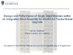
Ashley Greenall The University of Liverpool On behalf of the ATLAS Tracker Silicon Strip Upgrade Stave Programme 1 Outline Topical Workshop on Electronics for Particle Physics Aachen September 2024 2010 ID: 780715
Download The PPT/PDF document "Design and Performance of Single-Sided M..." is the property of its rightful owner. Permission is granted to download and print the materials on this web site for personal, non-commercial use only, and to display it on your personal computer provided you do not modify the materials and that you retain all copyright notices contained in the materials. By downloading content from our website, you accept the terms of this agreement.
Slide1
Design and Performance of Single-Sided Modules within an Integrated Stave Assembly for the ATLAS Tracker Barrel Upgrade
Ashley
Greenall
The University of Liverpool
On behalf of the ATLAS Tracker Silicon Strip Upgrade Stave Programme
Slide21
Outline
Topical Workshop on Electronics for Particle Physics Aachen, September 20-24, 2010
Introduction to the Stave
concept
Stave flex hybridAssembly & Electrical performanceStave moduleAssembly & Electrical performanceFirst look at multi-module performanceSummary and outlook
Slide32
Topical Workshop on Electronics for Particle Physics Aachen, September 20-24, 2010
Introduction to the Stave
concept
Stave
flex hybridAssembly & Electrical performanceStave moduleAssembly & Electrical performanceFirst look at multi-module performanceSummary and outlook
Slide4Stave – Geometry and components
1200mm
Bus cable
Hybrid + Sensor
Carbon honeycomb
Carbon fiber
facing
Readout IC’s
P-type 4 segment crystals (
10cmx10cm
, 320µm thick)
4 blocks of 1280 strips, 5120 total
ABCN-25
readout ASIC
40 per module
960 per stave (>120k channels)
Kapton
flex hybrid with auxiliary boards
BCC ASIC (multi drop & point-to-point I/O
)
Serial Power
protection
Serial powering of modules
Embedded Kapton bus cable
End of stave card
Stave mechanical core
Coolant tube structure
3
Single flex
Module with 2 x flex
120mm
Sensor
12 modules/side of
stave (24 total)
Topical Workshop on Electronics for Particle Physics Aachen, September 20-24, 2010
Auxiliary Board(s)
Slide5Stave Module Requirements
4
Topical Workshop on Electronics for Particle Physics Aachen, September 20-24, 2010
Design is driven by minimising material
Hybrid is substrate-less and with no connectors
Glued directly on to the sensor Provides mechanical support and thermal managementAll off-module connections made via wire bonds
Use of minimal glue layers for both ASIC and hybrid attachment
Improves thermal paths and again reduces material
Pitch adapters not used, direct ASIC-to-Sensor wire bonding
Constrains relative placement w.r.t. sensor to better than 80µm
Layout optimised for Stave and Serial powering (parallel optional)
Scalable serial power connection (for multiple modules)
2.5V offset between hybrids (5V across a single module)
Opportunity to look at mass production methods (future build will require >10000 circuits)
Yield and reliability of flex circuits taken into account from the beginning
Mass wire bonding, component attachment and testing of circuits
Possible to implement techniques with minimum financial penalty (capital outlay etc.)?
Slide65
Topical Workshop on Electronics for Particle Physics Aachen, September 20-24, 2010
Introduction to the Stave
concept
Stave
flex hybridAssembly & Electrical performanceStave moduleAssembly & Electrical performanceFirst look at multi-module performanceSummary and outlook
Slide7Stave flex hybrid – Design for manufacture
5 layer flex using conservative design rules – maintains optimum volume/yield
100µm track and gap, blind
vias
(
375µm lands with 150µm drill) and 50µm dielectricsNon-esoteric design – relatively cheap to produceFirst pass at industrialisation of hybridsPanelisation of flexes – allows mass wire-bonding and testing of circuitsDesign for machine placement and solder re-flow of passive componentsMass attachment of bare die
6
Topical Workshop on Electronics for Particle Physics Aachen, September 20-24, 2010
Panel is composed of 8 ‘active’ circuits
Flexi-rigid build
5 layer flex selectively laminated to FR4
Flex is 4 active layers + shield (asymmetric stack up)
FR4 acts as temporary substrate during assembly
Panel dimension is 300mm x 200mm
Geometry determined by pick-n-place machine
Flex active circuit is 24mm x 107.6mm
It is this which is detached from the panel
Completed circuits are electrically tested on the panel
After component attachment and wire bonding
Vendors yield, of panel, is >96%
Slide8Panel Details
Lamination of Kapton flex to FR4 incurs shrinkage
Typically 1.5mm over 300m and 0.5mm over 200mm (x and y respectively)
Machine placement of passives difficult and incurs solder stencil misalignment
Complication of some panel tooling holes having to track shrinkage – challenging for vendor
Requires a 2nd run with shrinkage correction input at CAM stageShrinkage now well controlled at ≤50µm for both x and y
7
Topical Workshop on Electronics for Particle Physics Aachen, September 20-24, 2010
Circuits are laser cut on 4 sides
4 tabs, 1 per corner, used to retain circuit(s)
No bond ply beneath circuit
Use non-flexible solder resist (25µm thickness)
Improved registration (compared to flexible resist)
Adds rigidity to circuit
Cu dot hatch added by vendor
Makes lamination of flex to FR4 more uniform (& plating)
BUT dots are ~40µm high
w.r.t
.
Kapton
carrier
Introduces non-uniformity in glue layer when attaching die (aim for ~80µm glue thickness)
Solution was to add ‘landing pads’ for chip placement and hybrid pick up tool (
Flatness of landing pads
w.r.t
. ASIC sites is ~10µm
)
Tabs
Landing Pads
Laser cut
Slide9ASIC ‘Mass’ Attachment
Attach 20 x ASICs to a single hybrid (on a panel) at a time
,
using conductive glue
Important to control chip-to-chip alignment to better than 80µm and maintain their planarity to 10µm
Constraint on planarity necessary as we pick up the completed hybrid via the chip faces when gluing to the sensor - at this stage the hybrid will be ‘flexible’ (due to having no substrate) and is wire bonded.Make use of a ‘chip-tray’ (pre-load with ASICs) - geometry matches that of the ASIC sites on the hybridMade from Acetal (Static Dissipative), with a 125µm thick laser cut stencil added for precision alignment of ASICsAll ASICs picked up in one step from the tray using a vacuum pickup tool and then have glue applied
Again using a 125µm thick stencil (cut to match glue profile) and ensure uniform glue thickness applied
Then ready to attach all 20 x ASICs in one go to the flex
8
Topical Workshop on Electronics for Particle Physics Aachen, September 20-24, 2010
Slide10Component Attachment and wire bonding – Finished item
Pick-n-place and reflow of passives on a panel is straightforward (as a normal FR4 circuit)
Chip-to-chip placement (within a column) is <15µm RMS of requirement
Column-to-column placement is <20µm RMS
Glue thickness is very uniform with chip planarity <10µm
No evidence of wicking of glue from undersides of ASICsNo problems with wire-bonding of ASICs on flexes – vacuumed down during this stageHesse & Knipps Bondjet BJ710 & BJ820 (10 minutes/flex for 20 ASICs on the 820)
9
Topical Workshop on Electronics for Particle Physics Aachen, September 20-24, 2010
9.6mm ±40µm
15.3mm ±100µm
Slide11Stave Hybrid – Layout and Electrical Detail
Hybrid is designed to accommodate 20 x ABCN-25 readout ASICs (2 columns of 10)
Layout topology matches ATLAS07 large area sensor and serially powered Bus cable
ASICs placed to match sensor pitch and bond pad profile
Hybrid Power and Digital I/O bond fields at opposite ends
Circuit exploits features of ABCN-25Bi-directional data paths
Embedded distributed shunt regulators (for serial powering)
Requires external control circuit
10
Topical Workshop on Electronics for Particle Physics Aachen, September 20-24, 2010
Mshunt
control and Digital I/O
Hybrid Power and sensor HV filtering
(
spec’d
to 500V)
Slide12Stave Hybrid – Electrical Performance
11
Topical Workshop on Electronics for Particle Physics Aachen, September 20-24, 2010
Characterisation of 10 x ABCN-25
Input
Noise ≤400e-Hybrids are tested for functional and electrical performance whilst on the panel
Check that shunt regulators work
Can alternatively be powered in ‘traditional’ parallel mode (bench PSU or DCDC for example)
Testing of bi-directional data paths (4 data paths total per hybrid)
Input noise, Gain and threshold variation
Input noise ≤400e ENC
Gain ~110mV/
fC
Threshold variation ~
1mV
Shunt Regulation
Readout Topology
Mshunt
characteristic for single and dual shunts enabled per ABCN-25 on a 20 ASIC hybrid
(expect max. Hybrid shunted current to be ≤5A)
Slide1312
Topical Workshop on Electronics for Particle Physics Aachen, September 20-24, 2010
Introduction to the Stave
concept
Stave
flex hybridAssembly & Electrical performanceStave moduleAssembly & Electrical performanceFirst look at multi-module performanceSummary and outlook
Slide14Stave Module Assembly
Completed (substrate-less) hybrids have to be detached from the panel
Whilst maintaining integrity of circuit (no damaged wire bonds etc.)
Solution is to use the same vacuum pickup tool as was used for ASIC attachment
With panel vacuum applied, hybrid retaining tabs are cut and then pickup tool attached
Apply vacuum to pickup tool and then release panel vacuum – circuit can then be lifted away13Topical Workshop on Electronics for Particle Physics Aachen, September 20-24, 2010
Module Assembly steps
Make use of jig (with precision dowels and
Kapton
barrier) plus PCB frame.
With sensor in place, glue applied using 80µm thick paper stencil (glue compressed to ~40µm after assembly).
Ready to attach the flex to the sensor.
Place in position and leave to cure (repeat process for the second hybrid).
After completion, then go for wire-bonding (whilst in frame).
Glue used for attaching hybrid to sensor is
Epolite
FH-5313 (electrical grade epoxy)
Samples irradiated at CERN PS to 9.3x10
14
n
eq
cm
-2
show no anomalous behaviour
Slide15Two test scenarios:
Test module with parallel powering - used as reference measurement
Both hybrids DC-referenced to sensor (and each other)
Serially powered
2.5V per hybrid, ~5V total across the module (using constant current source)
One hybrid is DC referenced to sensor, the other ACUse BCC ASICs for digital communication (AC-coupled LVDS), powered from hybrid14
Topical Workshop on Electronics for Particle Physics Aachen, September 20-24, 2010
Stave Module – Electrical Performance
Slide16Stave Module – Electrical Performance
15
Topical Workshop on Electronics for Particle Physics Aachen, September 20-24, 2010
Column 0
Parallel Powered (reference)
Serially PoweredSerially Powered Module Works!
Input Noise comparable between powering schemes
Evidence of a noise signature seen on module(s)
Outer columns have higher noise compared to inner
Irrespective of powering scheme
Column 1
Column 2
Column 3
Column 0
Column 1
Column 2
Column 3
Slide17Stave Module – Noise Signature
16
Topical Workshop on Electronics for Particle Physics Aachen, September 20-24, 2010
Inner column strips have consistently lower noise compared to outer strips (~20e to 30e less)
Assumed it was an artefact of serial powering – but also seen with parallel powered module(s)
Geometry of module - hybrids are attached asymmetrically on column boundary of sensorOuter strips have 15mm coverage by hybrid whilst the inner strip coverage is 9mmNoise appears to be anti-correlated to glue thickness
Small number of hybrids have had glue in-fill added to their columns – they show reduced noise
Points to increased load capacitance to ABCN-25 front-end from hybrid ground/shield
Nominal Thickness
Plot of estimated noise contribution from
shield as
f
unc
of glue thickness(scaled by inner
and outer strip coverage)
Data points added for noise measured from a
Module. Reasonable agreement with estimation
but evidence of glue thickness variation and tilt
in hybrid relative to sensor
Proposal is to either
Retain shield but increase glue layer to 100µm
Remove shield (further reduction of material)
Already done (yet to be tested)
Present build of 40µm glue layer, expect ~610e on inner strips and ~630e for outer strips
Slide18Short Stave Module Assembly – Stavelet
17
Topical Workshop on Electronics for Particle Physics Aachen, September 20-24, 2010
Stavelet: A test bed for serially powered multiple module studies
4 modules glued directly onto a stave assembly
Carbon structure with integrated coolingAuxiliary support electronics: Serial power control (e.g. bypass), module data I/O Integrated bus cableSerial power distribution, Sensor bias, Data I/O (multi-drop and point-to-point LVDS)
Serial Power Control (PPB)
Module Data I/O (BCC)
Slide19Short Stave Module Assembly – Stavelet
18
Topical Workshop on Electronics for Particle Physics Aachen, September 20-24, 2010
First Results
Input Noise ≤ 720e ENC
4 modules serially powered and readout at the same time8 hybrids, 16 data columns (mux’d
onto 8 data streams) – 160 ASICs (>20k channels)
First results look very promising
Slide20ATLAS Tracker Upgrade Week, 23rd-27th Feb 09
Summary & Outlook
Have successfully demonstrated the design and build of a substrate-less module
Issues of yield and volume production being addressed from the outset
Individually, serially powered modules, have been shown to perform excellently
First tests of a serially powered multi-module short stave (Stavelet) are very promisingStavelet tests are ongoing (with future plans for a DCDC powered variant)
Intention is to build a module using the new shield-less hybrids (reduced material)
Longer term, the plan is to build a full size double-sided Stave composed of 24 modules
Topical Workshop on Electronics for Particle Physics Aachen, September 20-24, 2010
20
Slide21ATLAS Tracker Upgrade Week, 23rd-27th Feb 09
Thank you!
Topical Workshop on Electronics for Particle Physics Aachen, September 20-24, 2010
20
Slide22ATLAS Tracker Upgrade Week, 23rd-27th Feb 09
Back up
Topical Workshop on Electronics for Particle Physics Aachen, September 20-24, 2010
21
Noise
contribution from shield
Assume capacitance to shield
in
same manner as to sensor backplane
Take sensor backplane capacitance 0.26 pF/cm and ratios of sensor and glue + solder resist thicknesses (310 mm
vs
25 mm + glue) and dielectric constant (11.4
vs
4.1) to get estimated load capacitance from shield layer per cm
Scale by coverage of inner and outer strips
To calculate noise take expected noise slope (80 e
-
/pF) and measured noise for double-sided module
Nominal Thickness
Estimate for nominal glue
of 40 µm
expect ~610
e
on inner strips and ~630
e
on outer strips