PDF-Manufacturing Processes for Engineering Materials, 5th ed.
Wafers and Chips
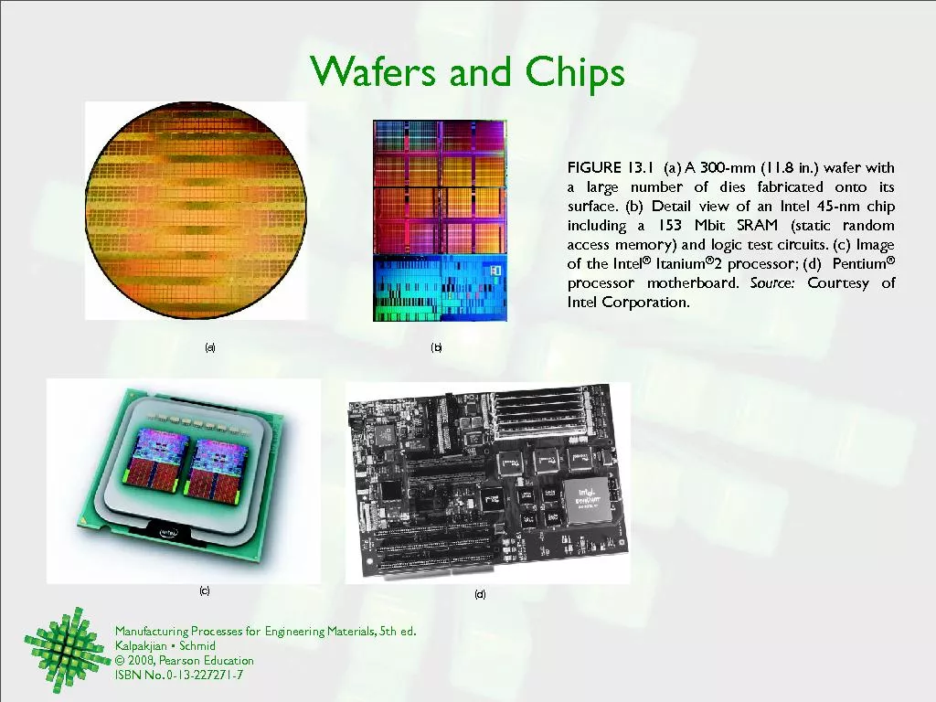
FIGURE 131 a A 300mm 118 in wafer with a large number of dies fabricated onto its surface b Detail view of an Intel 45nm chip including a 153 Mbit
Download Presentation
"Manufacturing Processes for Engineering Materials, 5th ed. " is the property of its rightful owner. Permission is granted to download and print materials on this website for personal, non-commercial use only, provided you retain all copyright notices. By downloading content from our website, you accept the terms of this agreement.
Presentation Transcript
Transcript not available.