/
Analog Applications Journal Understanding output voltage limitations of DCDC buck converters Analog Applications Journal Understanding output voltage limitations of DCDC buck converters

Analog Applications Journal Understanding output voltage limitations of DCDC buck converters - PDF document

olivia-moreira
olivia-moreira . @olivia-moreira
Follow
545 views
Uploaded On 2014-12-25

Analog Applications Journal Understanding output voltage limitations of DCDC buck converters - PPT Presentation

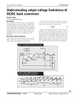
These operating ranges may be broad and in some cases may overlap It is usually not possible to derive any arbitrary output voltage from the entire range of permissible input voltages There are several factors that can cause this including the inter ID: 29265

These operating ranges may

Share:

Link:

Embed:

Download Presentation from below link

Download Pdf The PPT/PDF document "Analog Applications Journal Understandin..." is the property of its rightful owner. Permission is granted to download and print the materials on this web site for personal, non-commercial use only, and to display it on your personal computer provided you do not modify the materials and that you retain all copyright notices contained in the materials. By downloading content from our website, you accept the terms of this agreement.


Presentation Transcript

11Analog Applications JournalUnderstanding output voltage limitations ofDC/DC buck convertersIntroductionProduct datasheets for DC/DC converters typically showan operating range for input and output voltages. These 2Q 2008www.ti.com/aaj Comparator + RampGenerator +–+ Figure 1. Theoretical, ideal buck converter put voltage of the error amplifier. The output of the error OUT ErrorAmplifierDutyCyclePWMRamp Figure 2. Typical PWM waveforms at duty-cycle extremes and midpoint Texas Instruments Incorporated 12Analog Applications Journal www.ti.com/aaj2Q 2008switch, and the output voltage is 0 V. If the error-amplifierthe input voltage. For error-amplifier outputs betweenFor the ideal buck converter, any output voltage from 0 V. Normally, a resistor divider network asfier. This voltage is compared to Vstate regulation, the error-amplifier output will not goAs R2 approaches infinity, the output voltage goes tois the switching frequency.. Typically, if there is a VVDOUTIN(max)max VtVfOUTonINs(min)(min)=×× OUTREF VDVOUTIN inductor. Taking these losses into account, we can nowthe denominator, the duty cycle increases with increasingthe limiting factor, maximum duty cycle, is specified as aexample, the input-voltage range is 20 to 28 V, and theload current required is 2 to 3 A. Table 1 shows typicaldatasheet characteristics of the DC/DC converter. VDVIrrOUTINOUTDSDSOUT(max)max(min)(max)(max)[()]]=׊׊()].DSL VtfVIOUTonsINOUTDSDS(min)(min)(max)(max)(min))()=×׊][()].(min)Š×+IrROUTDSL VIrRVIrrOUTOUTDSLINOUTDSDS+×+Š×Š PARAMETER MINIMUM NOMINAL MAXIMUM Reference Voltage (V) -- 1.221 -- Switching Frequency (kHz) 400 500 600 Minimum Controllable ON Time (ns) -- 150 200 Maximum Duty Cycle (%) 87 -- -- FET rDS(on)(VIN)() -- 150 -- FET rDS(on)(VIN= 10 to 30 V) (m) -- 100 200 Table 1. Typical datasheet characteristics of DC/DC converter Texas Instruments Incorporated 13Analog Applications Journal 2Q 2008www.ti.com/aaj= 28 V, and Iwe use the appropriate specifications from Table 1. We alsoneed to supply the series resistance of the output inductor.To calculate the maximum output voltage, we need to= 200 mW, V= 20 V, I= 25 mW. With these values,Equation 8becomeschronous buck regulator. If both switches are internal tothe converter’s integrated circuit, they will likely have thefor the nonsynchronous buck converter, the minimum andIf the diode forward-voltage drop is 0.4 V, then for the VDVIrVOUTINOUTDSdOUT(max)max(min)(max)(max)[()]=׊׊ VtfVIOUTonsINOUTDSd(min)(min)(max)(max)(min))()]=×׊׊Š(((min)IRVOUTLd OUT(max).[(..)][(..)]=׊׊Š×+087203020230202516725 V OUT(min)[(..)][(..)]=×׊׊Š×+200600282010120100253306 . ages would be 2.838 V and 18.525 V, respectively. Thedown to 0 V, practical limita-Additionally, real-world circuits contain losses. These lossesand may be used to one’s advantage when output-voltagepower.ti.com IMPORTANT NOTICE Texas Instruments Incorporated and its subsidiaries (TI) reservestandard warranty. Testing and other quality control techniques areused to the extent TI deems necessary to support this warranty.applications using TI components. To minimize the risksunder the patents or other intellectual property of the third party, or aTexas Instruments products and application solutions: TIWorldwide Technical Support InternetTI Semiconductor Product Information Center Home Pagesupport.ti.comTI Semiconductor KnowledgeBase Home Pagesupport.ti.com/sc/knowledgebase Phone+1(972) 644-5580Fax+1(972) 927-6377 Internet/Emailsupport.ti.com/sc/pic/americas.htmEuropean Free Call00800-ASK-TEXASInternational+49 (0) 8161 80 2121Russian Support+7 (4) 95 98 10 701The European Free Call (Toll Free) number is not active in all countries. If you havetechnical difficulty calling the free call number, please use the international number above.Fax+(49) (0) 8161 80 2045 International+81-3-3344-5317Domestic0120-81-0036Internationalsupport.ti.com/sc/pic/japan.htm Domesticwww.tij.co.jp/picInternational+886-2-23786800DomesticToll-Free NumberToll-Free NumberAustralia1-800-999-084Malaysia1-800-80-3973China800-820-8682New Zealand0800-446-934Hong Kong800-96-5941Philippines1-800-765-7404India+91-80-41381665 (Toll)Singapore800-886-1028Indonesia001-803-8861-1006Taiwan0800-006800Korea080-551-2804Thailand001-800-886-0010Fax+886-2-2378-6808Emailtiasia@ti.comInternetsupport.ti.com/sc/pic/asia.htmti-china@ti.com of similar import. Similarly, such statements herein that describethe company's products, business strategy, outlook, objectives,of operations. We disclaim any intention or obligation to updateTrademarks: Mailing Address: Texas InstrumentsDallas, Texas 75265 Texas Instruments Incorporated Telephony Video & Imaging www.ti.com/wireless SLYT