/
MT TUTORIAL Op Amp Input Bias Current DEFINITION OF INPUT BIAS CURRENT Ideally no current MT TUTORIAL Op Amp Input Bias Current DEFINITION OF INPUT BIAS CURRENT Ideally no current

MT TUTORIAL Op Amp Input Bias Current DEFINITION OF INPUT BIAS CURRENT Ideally no current - PDF document

phoebe-click
phoebe-click . @phoebe-click
Follow
666 views
Uploaded On 2015-03-15

MT TUTORIAL Op Amp Input Bias Current DEFINITION OF INPUT BIAS CURRENT Ideally no current - PPT Presentation

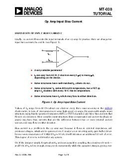
In practice there are always two input bias currents I B and I B see Figure 1 Rev0 1008 WK Page 1 of 5 A very variable parameter B can vary from 60 fA 1 electron every 3 s to many A depending on the device Some structures have wellmatched I others ID: 46094

practice there are

Share:

Link:

Embed:

Download Presentation from below link

Download Pdf The PPT/PDF document "MT TUTORIAL Op Amp Input Bias Current DE..." is the property of its rightful owner. Permission is granted to download and print the materials on this web site for personal, non-commercial use only, and to display it on your personal computer provided you do not modify the materials and that you retain all copyright notices contained in the materials. By downloading content from our website, you accept the terms of this agreement.


Presentation Transcript

Op Amp Input Bias Current DEFINITION OF INPUT BIAS CURRENT Ideally, no current flows into the input terminals of an op amp. In practice, there are always two +– IB+IB- electrometer, to tens of microamperes in some high speed op amps. Op amps with simple input ansistors (BJT) or FET long-taileflow in one direction. More complex input structures (bias-compensated and current feedback op amps) may have bias currents that are the diffe MT-038 more misleading results. The moral here, in any op amp circuit. The same admonition goes for in-amp circuits. INPUT OFFSET CURRENT , is the difference between Iis only meaningful where the two individual bias currents are fundamentally reasonably well-matched, to begin with. This is true for most voltage feedback (VFB) op amps. However, it wouldn't for example be meaningful to speak of I for a current feedback (CFB) op amp, as the currents are radically un-matched. It should be noted that rail-to-rail input stages comprised have bias currents common-mode voltage passes through offset currents for these devices are especially difficult to specmaximum positive/negative value. INTERNAL BIAS CURRENT CANCELLATION CIRCUITS external current then flowing in the input terminbase current and the current source, which can be quite small. Low Offset Voltage: As low as Low Offset Drift: As low as Temperature Stable IbiasLow Bias Currents: -10nALow Voltage Noise: As low as Poor Bias Current Match (Currents May Even Flow in Opposite Directions)Higher Current NoiseNot Very Useful at HFMatching source impedances makes offset error due to bias current worse because of additional impedance Figure 2: A Bias Current Compensated Bipolar Input Stage Page 2 of 5 MT-038 Most modern precision bipolar input stage op amps use some means of internal bias current compensation, examples would be the familiar OP27 Bias current compensated input stages have mainput stage, namely: low voltage noise, low offsbias current which is fairly stable with tempergood, and their bias current matching is poor. from the external bias current being the differencebetween the compensating current source and the icorrelated, the two noises add in a root-sum-of-Since the resulting external bias current is the difference between two nearly equal currents, currents of a bias-compensated op amp may not only be mismatched, they can actually flow in ations this isn't imporeffects (for example the droop of a sample-and-hold (SHA) built with a bias-compensated op amp may have either polarity). In many cases, the bias current compensation feature is not mentioned on an op amp data sheet, and a simplified schematic isn't supplied. It is easy to determine if bias current compensation is used by examining the bias current specification. If the bias current is specified as a "the op amp is most likely compensated for bias current. Note that this can examining the offset current specification (the difference in the bias currents). If internal bias current compensation exists, the offset current will be of the same magnitude as the bias current. Without bias current compensation, the offset curresmaller than the bias current. Note that these relationships generally hold, regardless of the exact magnitude of the bias currents. As previously mentioned, rail-to-raicommon-mode voltage passes through the transition region. Bias and offset currents for these devices are especially difficult to specify, other than simply giving a maximum positive/negative CANCELING THE EFFECTS OF BIAS CURRENT (EXTERNAL TO THE OP AMP) tched (the case with simpop amps, but internally bias compensated ones, as noted previously), a bias compensation rting input to match and thus compensate the drop in the parallel combination of R1 and R2 in the inverting input. This minimizes additional offset voltage error, as in Figure 3. Note that if R3 is more than 1 kit should be bypassed with a capacitor to prevent noise pickup. Also note that this form of bias cancellation is useless where bias currents are not well-matched, and will, in fact, make matters Page 3 of 5 MT-038 –+ R3 = R1 || R2 IB–IB+ = R2 (I= R2 I= 0, IF INEGLECTING V ffects of Input Bias CurrentMEASURING INPUT OFFSET AND INPUT BIAS CURRENT Input bias current (or input offset voltage) may be measured using the test circuit of Figure 4. To measure I, a large resistance, Rapparent additional offset voltage equal to I has previously been measured can be determined, and I is then easily computed. This yields values for I is the average of values vary from 100 k for bipolar op amps to 1000 M –+ RS RS 100100 DUT –+ VO 10k �� 100(100kTO 1GS1 CLOSED TO TEST IS2 CLOSED TO TEST IBOTH CLOSED TO TEST VBOTH OPEN TO TEST I= 1 + 100 100 100 1 ++–VOSIB+RSIB-RS Figure 4: Measuring Input Bias Current Page 4 of 5 Extremely low input bias currents must be measura capacitor, and the rate of voltage change is measured. If the capacitor and general circuit leakage is negligible the current may be calculated directly from the rateFigure 5 below illustrates the general concept. With one switch open and the opposite closed, either I is measured. –+ VO DUT C S1VOt =IBC IB=CVOt OPEN S1 TO MEASURE IOPEN S2 TO MEASURE I Figure 5: Measuring Very Low Bias Currents It should be obvious that only a premium capacitor dielectric can be used for C, for example REFERENCES: Hank Zumbahlen, Basic Linear Design, Analog Devices, 2006, ISBN: 0-915550-28-1. Also available as Linear Circuit Design Handbook , Elsevier-Newnes, 2008, ISBN-10: 0750687037, ISBN-13: 978-0750687034. Chapter 1. Walter G. Jung, Op Amp Applications Analog Devices, 2002, ISBN 0-916550-26-5, Also available as Amp Applications Handbook , Elsevier/Newnes, 2005, ISBN 0-7506-7844-5. Chapter 1. Copyright 2009, Analog Devices, Inc. All rights reserved. Analog Devices assumes no responsibility for customer product design or the use or application of customers’ products or for any infringements of patents or rights of others which may result from Analog Devices assistance. All trademarks and logos are property of their respective holders. Information furnished by Analog Devices applications and development tools engineers is believed to be accurate and reliable, however no responsibility is assumed by Analog Devices regarding technical accuracy and topicality of the content provided in Analog Devices Tutorials. Page 5 of 5