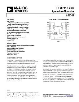
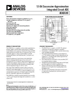
/
REV A Information furnished by Analog Devices is believed to be accurate and reliable REV A Information furnished by Analog Devices is believed to be accurate and reliable

REV A Information furnished by Analog Devices is believed to be accurate and reliable - PDF document

phoebe-click
phoebe-click . @phoebe-click
Follow
543 views
Uploaded On 2014-12-28

REV A Information furnished by Analog Devices is believed to be accurate and reliable - PPT Presentation

A Information furnished by Analog Devices is believed to be accurate and reliable However no responsibility is assumed by Analog Devices for its use nor for any infringements of patents or other rights of third part ID: 30452

Information furnished

Share:

Link:

Embed:

Download Presentation from below link

Download Pdf The PPT/PDF document "REV A Information furnished by Analog De..." is the property of its rightful owner. Permission is granted to download and print the materials on this web site for personal, non-commercial use only, and to display it on your personal computer provided you do not modify the materials and that you retain all copyright notices contained in the materials. By downloading content from our website, you accept the terms of this agreement.


Presentation Transcript

ADM8828/ADM8829Ð4Ð REV. I OUT 1015202530354045 PEFF @ VIN = 2.0V PEFF @ VIN = 3.3V PEFF @ VIN = 5.0V Figure 8.Power Efficiency vs. Output Current Ð50125Ð10102540608090110 RESISTANCE (V) @ VIN = 1.5V RESISTANCE (V) @ VIN = 3.3V Figure 9.Output Resistance vs. Temperature Ð10102540608090110 PUMP FREQUENCY@ VIN = 5.0V PUMP FREQUENCYIN = 3.3V Figure 10.Charge Pump Frequency vs. Temperature ADM8828/ADM8829Ð3Ð REV. Typical Performance CharacteristicsÐ 15.522.533.544.55 Figure 2.Power Supply Current vs. Voltage 1.55.52.533.544.55 Figure 3.Output Source Resistance vs. Supply Voltage CAPACITANCE Ð mF201800.473.31OUTPUT CURRENT Ð mA2.28212101614 OUTPUT CURRENT @ VIN = 4.75V OUTPUT CURRENT @ VIN = 3.15V Figure 4.Output Current vs. Capacitance CAPACITANCE Ð mF605000.473.31OUTPUT VOLTAGE RIPPLE Ð mV p-p2.24010 OUTPUT VOLTAGE RIPPLE@ VIN = 4.75V OUTPUT VOLTAGE RIPPLEIN = 3.15V OUTPUT VOLTAGE RIPPLEIN = 1.9V IL = 5mA Figure 5.Output Voltage Ripple vs. Capacitance CAPACITANCE Ð mF35030000.473.31OUTPUT VOLTAGE RIPPLE Ð mV p-p2.220010050250 OUTPUT VOLTAGE RIPPLE@ VIN = 1.9V, VOUT = Ð1.5V OUTPUT VOLTAGE RIPPLEIN = 4.75V, VOUT = Ð4.0V OUTPUT VOLTAGE RIPPLEIN = 3.15V, VOUT = Ð2.5V Figure 6.Output Voltage Ripple vs. Capacitance 10152025303540 OUTPUT VOLTAGE @ VIN = 2.0V OUTPUT VOLTAGE @ VIN = 3.3V OUTPUT VOLTAGE @ VIN = 5.0V Figure 7.Output Voltage vs. Output Current Ð2Ð REV. ADM8828/ADM8829ÐSPECIFICATIONS MinTypMaxUnitsTest Conditions/Comments Input Voltage, IN1.55.5VRL = 10 kW 6001000AUnloaded1828Output Ripple25mV p-pI mV p-pICharge-Pump Frequency50120190kHz kHzVPower Efficiency90%R87%R99.599.96No Load 0.022ASHDN = IN Shutdown Exit Time175msIL = 5 mANOTES1C1 and C2 are low ESR (W) electrolytic capacitors. High ESR will degrade performance.Specifications subject to change without notice. InputVoltage (IN to GND) . . . . . . . . . . . . . . . Ð0.3 V to +6 VOUT to GND . . . . . . . . . . . . . . . . . . . . . . . .Ð6.0 V to +0.3 VOUT, IN Output Current (Continuous) . . . . . . . . . . . . 50 mAOutput Short Circuit Duration to GND . . . . . . . . . . . 10 secsPower Dissipation, RT-6 . . . . . . . . . . . . . . . . . . . . . . 570 mW, Thermal Impedance . . . . . . . . . . . . . . . . . . . . 120Industrial (A Version) . . . . . . . . . . . . . . . . Ð40Storage Temperature Range . . . . . . . . . . . Ð65Lead Temperature Range (Soldering10sec) . . . . . . . . +300Vapor Phase (70 sec) . . . . . . . . . . . . . . . . . . . . . . . . +215Infrared (15 sec) . . . . . . . . . . . . . . . . . . . . . . . . . . . . +220ESD Rating . . . . . . . . . . . . . . . . . . . . . . . . . . . . . . . . �3500 V TOP VIEW(Not to Scale) OUTINCAPÐCAP+SHDNADM882816 TOP VIEW(Not to Scale) OUTINCAP+ADM882916CAPÐNC = NO CONNECTPIN FUNCTION DESCRIPTIONS MnemonicFunctionSHDNShutdown Control Input. This input, when INPositive Power Supply Input. ADM8828/ADM8829Ð5Ð REV. on-chip oscillator and switching network transfers charge between Figure 11.Voltage Inversion Principlelogic high level on the SHDN input shuts the device downreducing the quiescent current to 0.02 Reducing the ESR reduces the output impedance and ripple.provide instantaneous current surges as required. Suitable capaci-tors of 1 Figure 12.Typical Circuit Configuration a ADM8828ADM8829 Rel8 581.127.2500 ©1777–2017Analog Bevices, Inc. All rights reserved. Switched-CapacitorVoltage Inverter with ShutdownFUNCTIONAL BLOCK DIAGRAMS TOP VIEW(Not to Scale) OUTINCAPÐCAP+SHDNADM882816 TOP VIEW(Not to Scale) inverting scheme is ideal for generating a needed for the charge pump. Output currents up to 25 mA withcent current to 20nA. Figure 1.Typical Circuit Configuration ADM8828/ADM8829 Data Sheet Rev. B | Page 6 of 7 COMPLIANTTOJEDECSTANDARDSMO-178-AB 12° SEATINIPLANE 10922095BSC2082 502220922082 502220822082 107210821052 105210152092 015MA; 025MIN 1045MA;2095MIN 2022MA;2028MIN 2052MA;2052MIN 205520452055 PIN1INDICATOR 12-18-2228-AFigure 13. 6-Lead Small Outline Transistor Package [SOT-23] (RJ-6) Dimensions shown in millimeters ORDERING GUIDE Temperature Range Package Description Package Option Marking Code ADM8828ARTZ-REEL7 Š40°C to +85°C 6-Lead Small Outline Transistor Package [SOT-23] RJ-6 MM0 ADM8829ARTZ-REEL Š40°C to +85°C 6-Lead Small Outline Transistor Package [SOT-23] RJ-6 MN0 ADM8829ARTZ-REEL7 Š40°C to +85°C 6-Lead Small Outline Transistor Package [SOT-23] RJ-6 Z = RoHS Compliant Part. Data Sheet ADM8828/ADM8829 Rev. B | Page 7 of 7 REVISION HISTORY 3/19„Rev. A to Rev. B Updated Outline Dimensions ......................................................... 6 Changes to Ordering Guide ............................................................ 6 11/06„Rev. 0 to Rev. A ©1999…2019 Analog Devices, Inc. All rights reserved. Trademarks and registered trademarks are the property of their respective owners. D03352-0-3/19(B) Data Sheet ADM8828/ADM8829 Rev. B | Page 7 of 7 REVISION HISTORY 3/19„Rev. A to Rev. B Updated Outline Dimensions ......................................................... 6 Changes to Ordering Guide ............................................................ 6 11/06„Rev. 0 to Rev. A ©1999…2019 Analog Devices, Inc. All rights reserved. Trademarks and registered trademarks are the property of their respective owners. D03352-0-3/19(B) ADM8828/ADM8829 Data Sheet Rev. B | Page 6 of 7 COMPLIANTTOJEDECSTANDARDSMO-178-AB 12° SEATINIPLANE 10922095BSC2082 502220922082 502220822082 107210821052 105210152092 015MA; 025MIN 1045MA;2095MIN 2022MA;2028MIN 2052MA;2052MIN 205520452055 PIN1INDICATOR 12-18-2228-Aure 13. 6-Lead Small Outline Transistor Package [SOT-23] (RJ-6) Dimensions shown in millimeters ORDERING GUIDE Temperature Range Package Description Package Option Marking Code ADM8828ARTZ-REEL7 Š40°C to +85°C 6-Lead Small Outline Transistor Package [SOT-23] RJ-6 M ADM8829ARTZ-REEL Š40°C to +85°C 6-Lead Small Outline Transistor Package [SOT-23] RJ-6 MN0 ADM8829ARTZ-REEL7 Š40°C to +85°C 6-Lead Small Outline Transistor Package [SOT-23] RJ-6 Z = RoHS Compliant Part. a ADM8828ADM8829 Rel8 581.127.2500 ©1777–2017Analog Bevices, Inc. All rights reserved. Switched-CapacitorVoltage Inverter with ShutdownFUNCTIONAL BLOCK DIAGRAMS TOP VIEW(Not to Scale) OUTINCAPÐCAP+SHDNADM882816 TOP VIEW(Not to Scale) inverting scheme is ideal for generating a needed for the charge pump. Output currents up to 25 mA withcent current to 20nA. Figure 1.Typical Circuit Configuration Data Sheet ADM8828/ADM8829 Rev. B | Page 7 of 7 REVISION HISTORY 3/19„Rev. A to Rev. B Updated Outline Dimensions ......................................................... 6 Changes to Ordering Guide ............................................................ 6 11/06„Rev. 0 to Rev. A ©1999…2019 Analog Devices, Inc. All rights d. Trademarks and Data Sheet ADM8828/ADM8829 Rev. B | Page 7 of 7 REVISION HISTORY /19„Rev. A to Rev. B Updated Outline Dimensions ......................................................... 6 Changes to Ordering Guide ............................................................ 6 11/06„Rev. 0 to Rev. A ©1999…2019 Analog Devices, Inc. All rights d. Trademarks and