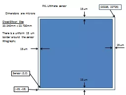
20235 22725 PXL Ultimate sensor Diced Silicon Size 20240mm x 22730mm There is a uniform 15 um border around the sensor lithography 15 um 15 um 15 um 15 um 15 15 Dimensions are microns ID: 465557
Download Presentation The PPT/PDF document "Sensor (0,0)" is the property of its rightful owner. Permission is granted to download and print the materials on this web site for personal, non-commercial use only, and to display it on your personal computer provided you do not modify the materials and that you retain all copyright notices contained in the materials. By downloading content from our website, you accept the terms of this agreement.
Slide1
Sensor (0,0)
(20235, 22725)
PXL Ultimate sensor
Diced Silicon Size
20.240mm x 22.730mm
There is a uniform 15 um border around the sensor lithography
15 um
15 um
15 um
15 um
(-15, -15)
Dimensions are micronsSlide2Slide3
Optical fiducial point locations are shown on the next pagesSlide4
Right side
Left sideSlide5
Right SideSlide6
Right Side
This corner
X= 18165.075 µm
Y= 871.6 µmSlide7
Left SideSlide8
Left Side
This corner
X= 4594.225 µm
Y= 920.775 µmSlide9
Cable sizes and locations of sensorsSlide10
Ladder end detail
3.1 mm
Sensors are aligned to the upper edge of the cableSlide11
214.48 mm
1 mm gap
Low mass sensor section
Driver section
91.02 mm
Total length = 306.5 mm
Width = 24.43 mm Slide12
Joe Silber - Attached are measurements I made yesterday.1) If I divide the total width of 10 butted sensors by 10x Leo's
nominal width (19.62mm) I get an average gap of 2um.2) If I instead divide by the width I measured (19.607mm) then I getaverage gap of 16um.3) If I add up the worst cases of offset and rotation that I measured,then the maximum
tol envelope would be 54um.4) If I add up the stdevs on offset and rotation that I measured, then
the tol envelope should be 18um.Clearly I may be simply interpreting the edge of sensor incorrectly
due to my lighting conditions. If so, then the average gap is is tiny,2um, as in case (1). But if I am seeing things correctly on thesmartscope, then this batch of sensors were cut undersized by about
13um on average, and the correct gap to model would be more like16-18um, as in cases (2) and (4). Case (3) is essentially what Howardoriginally assumed (2 mil), but in reality it looks to me like itwould be incorrect for us to assume this worst-case placement on every
sensor.I think the bottom line is that if Leo can stomach about 100um maximumerror for wire bond alignment, then we should be fine splitting the
difference between the 2 um and 18 um numbers, and calling the nominalgap 10um.Slide13
Gap detail
10 umSlide14
More background materialSlide15
CC - IPHC 8th March 2011 - ULTIMATE
ULTIMATERun SA35C11_1 # 12404
X (mm)
Y (mm)
Chip Size
20,240
22,730
Step Size
20,340
23,530
Scribeline
0,100
0,800
Possible Dies 48Slide16
CC - IPHC 8th March 2011 - ULTIMATETraceability – Chip NumberingSlide17
CC - IPHC 8th March 2011 - ULTIMATE
X (mm)
Y (mm)
Chip Size
20,240
22,730
Step Size
20,340
23,530
Scribeline
0,100
0,800
Possible Dies 48
Sawing Diagram