/
CONNECTING MINDS.ADVANCING LIGHT. CONNECTING MINDS.ADVANCING LIGHT.

CONNECTING MINDS.ADVANCING LIGHT. - PDF document

stefany-barnette
stefany-barnette . @stefany-barnette
Follow
576 views
Uploaded On 2016-06-19

CONNECTING MINDS.ADVANCING LIGHT. - PPT Presentation

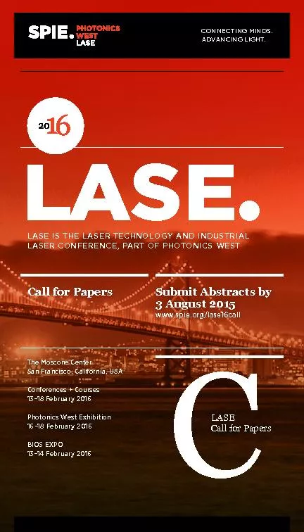
Call for Papers Submit Abstracts by3 August 2015 wwwspieorglase16call The Moscone CenterSan Francisco California USA C LASE LASE IS THE LASER TECHNOLOGY AND INDUSTRIAL LASER CONFERENCE PART OF P ID: 369581

Call for Papers Submit Abstracts by3

Share:

Link:

Embed:

Download Presentation from below link

Download Pdf The PPT/PDF document "CONNECTING MINDS.ADVANCING LIGHT." is the property of its rightful owner. Permission is granted to download and print the materials on this web site for personal, non-commercial use only, and to display it on your personal computer provided you do not modify the materials and that you retain all copyright notices contained in the materials. By downloading content from our website, you accept the terms of this agreement.


Presentation Transcript

CONNECTING MINDS.ADVANCING LIGHT. Call for Papers Submit Abstracts by3 August 2015 www.spie.org/lase16call The Moscone CenterSan Francisco, California, USA C LASE LASE IS THE LASER TECHNOLOGY AND INDUSTRIAL LASER CONFERENCE, PART OF PHOTONICS WEST LASE Call for Papers C.Call for Papers. DATESConferences + Courses: 13–18 February 2016LOCATIONThe Moscone CenterSan Francisco, California, USA Present your work at LASELASE conferences address the latest results in laser sources, materials, and engineering TECHNOLOGIESLaser Source EngineeringNonlinear OpticsSemiconductor Lasers and LEDsLaser Micro-/NanoengineeringLaser ApplicationsGreen Photonics3D Printing The Moscone CenterSan Francisco, California, USA DATESConferences & Courses: 13–18 Feburary 2016TWO EXHIBITIONSBiOS EXPO: 13–14 February 2016Photonics West: 16–18 February 2016 Participate in the premier technical event and marketplace for the photonics, biophotonics, and laser industry. BiOS –BiophotonicsTopics include biomedical optics, photonic therapeutics and diagnostics, tissue engineering, translational research, tissue optics, clinical technologies and systems, biomedical spectroscopy, microscopy, imaging, nano/biophotonics.LASE –Lasers and SourcesTopics include laser source engineering, nonlinear optics, semiconductor lasers and LEDs, laser manufacturing, laser micro-/nanoengineering, 3D fabrication, and more.OPTO – Optoelectronic Devices and MaterialsTopics include optoelectronic materials and devices, photonic integration, displays and holography, nanotechnologies in photonics, advanced quantum and optoelectronic applications, semiconductor lasers and LEDs, MOEMS-MEMS, optical communications: devices to systems.BiOS EXPO: The world’s largest biomedical optics and biophotonics exhibition. The exhibition had more than 220 companies in 2015.Photonics West Exhibition: The agship event for companies in the photonics industry. The exhibition sold out in 2015 with more than 1,250 companies.Present your work at Photonics West, the premier laser, photonics, biomedical optics conference: 20,000 attendees, two exhibitions, 1,250 exhibiting companies, a wide range of papers on biomedical optics, biophotonics, industrial lasers, optoelectronics, microfabrication, MOEMS-MEMS, displays, and more.Translational Research: Including the latest photonics technologies, tools, and techniques with high potential to impact healthcare.Green Photonics:Including green photonics for solid state lighting and displays, laser-assisted manufacturing and micro/nano fabrication, communications, renewable energy generation: fusion and photovoltaics.3D Printing: Highlighting papers from BiOS, LASE, and OPTO that showcase innovative ways to apply this multidimensional/multidisciplinary technology.If your BiOS, LASE, or OPTO paper has applications in translational research, 3D printing, environmental or energy solutions, then you are eligible to also submit your abstract to the Photonics West Application Tracks. Details provided in the online submission webpage. www.spie.org/lase16call \r 13–18 FEBRUARY 2016 SUBMIT YOUR ABSTRACT TODAY • The Moscone Center San Francisco, California, USA P.O. Box 10Bellingham, WA 98227-0010 USA The Moscone Center San Francisco, California, USA www.spie.org/lase16callPresent your research on �ber, solid state, diode, ultrafast, high power, VECSELs, semiconductor lasers and more. SPIE PHOTONICS WEST 2016 • www.spie.org/lase16call Start your sales year at the premier photonics and laser event.Experience Photonics West—your exhibition booth will put you face-to- face with over 20,000 attendees and over 1,250 exhibiting companies, plus you can access the world’s most comprehensive photonics and laser conference.There is no other event that provides your company the exposure of SPIE Photonics West. Every year more products are launched, more deals are made, and more collaboration occurs—it is the annual agship event for the photonics industry.Grow your revenueIdentify the hottest opportunities in the industryConnect with your customersDemo your new productsGain exposure with strategically placed advertising and sponsorshipsINTERESTED IN EXHIBITING, SPONSORING AN EVENT, ADVERTISING WITH SPIE OR TO LEARN MOREwww.spie.org/pwexhibition E. EXHIBITION“Photonics West was the best show ever! We started getting orders o the exhibition just a couple of weeks after the event. Great show, keep up the good work.”Brian Samoriski, President, Bristol Instruments, Inc. BiOS EXPO 13–14 Feb. 2016, the world's largest biomedical optics and biophotonics exhibition. BiOS EXPO, held Saturday and Sunday, kicks o the Photonics West week. Find the latest technologies from more than 220 companies in the thriving biomedical optics and photonics industries. PW Exhibition16-18 Feb. 2016 +1 360 676 3290 • help@spie.org • twitter (#PhotonicsWest)35 ABSTRACT SUBMISSIONAN AUTHOR OR COAUTHOR (INCLUDING KEYNOTE, INVITED, ORAL, AND POSTER PRESENTERS) WILL:Register at the reduced author registration rate(current SPIE Members receive an additional discount on the registration fee).Attend the meeting.Make the presentation as scheduled in the program.Submit a full-length manuscript (6 pages minimum) for publication in the SPIE Digital Library and Proceedings of SPIE.Obtain funding for registration fees, travel, and accommodations, independent of SPIE, through their sponsoring organizations.Ensure that all clearances, including government and company clearance, have been obtained to present and publish. If you are a DoD contractor in the USA, allow at least 60 days for clearance.Submit an abstract and summary online athttp://www.spie.org/lase16callAbstracts should contain enough detail to clearly convey the approach and the results of the research. Accepted abstracts will be published and made available at the meeting. Please submit a 250-word abstract for review.Please also submit a 100-word text summarysuitable for early release. If accepted, this summary text will be published prior to the meeting in the online or printed programs promoting the conference.Only original material should be submitted.Abstracts should contain enough detail to clearly convey the approach and the results of the research.Commercial papers, papers with no new research/development content, and papers where supporting data or a technical description cannot be given for proprietary reasons will not be accepted for presentation in this conference.Please do not submit the same, or similar, abstracts to multiple conferences.GREEN PHOTONICS: If your research is working toward improvements in energy, sustainability, and conservation, identify your paper as “GREEN” when prompted during the abstract submission wizard. If your paper is accepted, SPIE will contact you to collect a 1-2 page summary explaining how your research is “green.” If your paper is selected by Green Photonics selection committee, your presentation will be cross-listed in the SPIE Green Photonics Program, and you will be eligible to win an SPIE Green Photonics Best Paper Award.3D PRINTING: If your research is connected with 3D printing, manufacturing, or fabrication, enter “3D” when prompted during the abstract submission wizard. If your paper is accepted, SPIE will contact you to collect a 1-2 page summary explaining how your work can be used for an application area or can improve on current understandings. If your paper is selected by the 3D Printing committee, your presentation will be cross-listed in the SPIE Applications of 3D Printing Program and you will be eligible to win an SPIE Applications of 3D Printing Award.REVIEW, NOTIFICATION, AND PROGRAM PLACEMENT INFORMATIONTo ensure a high-quality conference, all submissions will be assessed by the Conference Chair/Editor for technical merit and suitability of content.Conference Chair/Editors reserve the right to reject for presentation any paper that does not meet content or presentation expectations.The contact author will receive notication of acceptance and presentation details by e-mail the week of 12 October 2015Final placement in an oral or poster session is subject to the Chairs’ discretion.PROCEEDINGS OF SPIE AND SPIE DIGITAL LIBRARY INFORMATIONManuscript instructions are available from the For Authors/Presenters” link on the conference website.Conference Chair/Editors may require manuscript revision before approving publication and reserve the right to reject for publication any paper that does not meet acceptable standards for a scientific publication. Conference Chair/Editors’ decisions on whether to allow publication of a manuscript is nal.Authors must be authorized to transfer copyright of the manuscript to SPIE, or provide a suitable publication license.Only papers presented at the conference and received according to publication guidelines and timelines will be published in the conference Proceedings of SPIE and SPIE Digital Library.Published papers are indexed in leading scientific databases including Astrophysical Data System (ADS), Chemical Abstracts (relevant content), Compendex, CrossRef, Current Contents, DeepDyve, Google Scholar, Inspec, Portico, Scopus, SPIN, and Web of Science Conference Proceedings Citation Index, and are searchable in the SPIE Digital Library. Full manuscripts are available to SPIE Digital Library subscribers worldwide. IMPORTANT DATESAbstracts Due:3 AUGUST 2015Author Notication:12 OCTOBER 2015Manuscript Due Date:20 JANUARY 2016Please Note: Submissions imply the intent of at least one author to register, attend the conference, present the paper as scheduled, and submit a full-length manuscript for publication in the conference proceedings. SPIE PHOTONICS WEST 2016 • www.spie.org/lase16call CALL FOR PAPERS CALL FOR PAPERS Symposium Chairs:Bruce TrombergBeckman Laser Institute, Univ. of California, Irvine (USA)Symposium Chair:Henry HelvajianThe Aerospace Corp. (USA) Symposium Chair:Stephen J. EglashStanford Data Science Initiative, Stanford Univ. (USA) If your BiOS, LASE, or OPTO paper has applications for translational research, 3D printing, environmental or energy solutions, then you are eligible to include your abstract in one of the Photonic West Applications Tracks. See details below on how to submit your abstract. TRANSLATIONALRESEARCHSPIE Translational Research 2016 will highlight papers from BiOS that showcase the latest photonics technologies, tools, and techniques with high potential to impact healthcare.GREEN PHOTONICSSPIE Green Photonics 2016 highlights papers from OPTO and LASE that showcase the latest photonics and optoelectronic tools and materials that will reduce power consumption, enable cleaner manufacturing, and create new energy generation for a broad range of applications.3D PRINTINGSPIE Applications of 3D Printing 2016 highlights papers from BiOS, LASE, and OPTO that showcase innovative ways to apply this multidimensional/multidisciplinary technology.Submit outcomes-based research in these areas:Laser-assisted Manufacturing and Micro/Nano FabricationRenewable Energy Generation: Fusion and PhotovoltaicsSolid State Lighting and DisplaysCommunicationsAdditive ManufacturingSelective Laser Melting, Maser Sintering, Laser PhotopolymerizationNovel Materials, Protean Materials, and Laser InteractionsSoftware that Increases Eciencies and SpeedIn-situ Sensors or Probes to Verify and Quantify Additive Manufacturing Processes in Real TimeConformal Photonics/ElectronicsSTEPS:SUBMIT YOUR ABSTRACT TODAY!www.spie.org/lase16callPhotonic Therapeutics and DiagnosticsTissue Optics, Laser-Tissue Interaction, and Tissue EngineeringClinical Technologies and SystemsBiomedical Spectroscopy, Microscopy, and ImagingNano/BiophotonicsNeurophotonics, Neurosurgery, and OptogeneticsGabriela ApiouHarvard Medical School, Wellman Ctr. for Photomedicine, Massachusetts General Hospital (USA)Choose your conference in BiOS, LASE, or OPTO.When submitting your conference abstract, enter related Applications Track (translational research, 3D printing, or green photonics).If paper is accepted in the conference, it will be cross-listed in the Applications Track of your choice in online and printed programs.To compete for a Best Paper Award in the Applications Track (optional), submit a 1-2-page summary when prompted by SPIE sta. +1 360 676 3290 • help@spie.org • twitter (#PhotonicsWest)33 CALL FOR PAPERSVENUEThe Moscone Center747 Howard StreetSan Francisco, CA 94103-3118 USASan Francisco is often called “Everybody’s Favorite City,” a title earned by its scenic beauty, cultural attractions, diverse communities, and world-class cuisine. Visitors rate the atmosphere and ambience as their top reason for visiting San Francisco. Measuring 49 square miles, this walkable city is dotted with landmarks like the Golden Gate Bridge, cable cars, and Alcatraz.REGISTRATIONSPIE Photonics West registration will be available October 2015All participants, including invited speakers, contributed speakers, session chairs, co-chairs, and committee members, must pay a registration fee. Authors, coauthors, program committee members, and session chairs are accorded a reduced symposium registration fee.Fee information for conferences, courses, a registration form, and technical and general information will be available on the SPIE website in October 2015.HOTEL INFORMATIONOpening of the hotel reservation process for SPIE Photonics West 2016 is scheduled for June 2015. SPIE will arrange special discounted hotel rates for SPIE conference attendees.The website will be kept current with any updates.STUDENT TRAVEL GRANTSA limited number of SPIE student travel grants will be awarded based on need. Applications must be received no later than 7 December 2015. Eligible applicants must present an accepted paper at this meeting. Oer applies to undergraduate/graduate students who are enrolled full-time and have not yet received their PhD.CLEARANCE INFORMATIONIf government and/or company clearance is required to present and publish your presentation, start the process now to ensure that you receive clearance if your paper is accepted.IMPORTANT NEWS FOR ALL VISITORS FROM OUTSIDE THE UNITED STATESFind important requirements for visiting the United States on the SPIE Photonics West website. There are new steps that ALL visitors to the United States need to follow.Online at: www.spie.org/visaSPIE International HeadquartersPO Box 10Bellingham, WA 98227-0010 USATel: +1 360 676 3290 / Fax: +1 360 647 1445help@spie.org / www.SPIE.orgSPIE Europe Oce2 Alexandra GateFfordd Pengam, Cardi, CF24 2SA UKTel: +44 29 2089 4747 / Fax: +44 29 2089 4750info@spieeurope.org / www.SPIE.org SPIE PHOTONICS WEST 2016 • www.spie.org/lase16call LASER APPLICATIONS The paper you present will live far beyond the conference roomAll proceedings from this event will be published in the SPIE Digital Library, promoting breakthrough results, ideas, and organizations to millions of key researchers from around the world.www.SPIEDigitalLibrary.org Helping engineers and scientists stay current and competitive (OE124)Conference Chairs: Richard I. Epstein, The Univ. of New Mexico (USA); Denis V. Seletskiy, Univ. Konstanz (Germany); Mansoor Sheik-Bahae, The Univ. of New Mexico (USA)Program Committee: Daniel A. Bender, Sandia National Labs. (USA); Steven Bowman, U.S. Naval Research Lab. (USA); Tal Eliezer Carmon, Technion-Israel Institute of Technology (Israel); Joaquín Fernández, Univ. del País Vasco (Spain); Thomas Fraser, Air Force Research Lab. (USA); Zameer Ul Hasan, Temple Univ. (USA); Raman Kashyap, Ecole Polytechnique de Montréal (Canada); Paul D. LeVan, Air Force Research Lab. (USA); Mauro Tonelli, Univ. di Pisa (Italy); Qihua Xiong, Nanyang Technological Univ. (Singapore)The laser cooling of solids and the related area of electroluminescent refrigeration and thermoelectric cooling have been advancing on many fronts. Work on the laser cooling of rare-earth doped solids has expanded to include materials comprised of ytterbium, thulium, erbium and dysprosium dopants in a variety of crystal and glass hosts. The quality of these cooling materials have has improved to the point that operating temperatures below 100 K have been demonstrated, approaching liquid nitrogen temperatures. Rare-earth-based cryogenic optical This conference of related interest is part of OPTO 2016 co-located at Photonics West, www.spie.org/optocall refrigerators may soon nd applications in cooling infrared cameras, low-noise electronics, high-purity germanium gamma ray spectrometers and high-temperature superconductors. The last couple of years have also witnessed the rst demonstration of laser cooling in semiconductors and cryogenic cooling by collisional redistribution of radiation and spontaneous Brillouin cooling in microcavities. Additionally, there has been great progress in cooling of small mechanical structures with radiation pressure and encouraging proposals for various implementations of Raman cooling. We encourage the submission of papers dealing with experimental, theoretical studies and the applications of optical refrigeration of solids, electroluminescent refrigeration, radiationally balanced lasers, and optomechanical cooling.In parallel to the developments in laser cooling of solids, the alternative solid-state cooling technology of thermoelectric cooling has also seen great experimental and theoretical progress, with recent proposals of possibility of deep cryogenic operation of Peltier coolers. This conference will serve as a venue to present and discuss novel research on both optical and electronic cooling of solids. +1 360 676 3290 • help@spie.org • twitter (#PhotonicsWest)31 CALL FOR PAPERS This conference of related interest is part of OPTO 2016 co-located at Photonics West, www.spie.org/optocall (OE123)Conference Chairs: Jesper Glückstad, Technical Univ. of Denmark (Denmark); David L. Andrews, Univ. of East Anglia (United Kingdom); Enrique J. Galvez, Colgate Univ. (USA)Program Committee: Robert R. Alfano, The City College of New York (USA); Cornelia Denz, Westfälische Wilhelms-Univ. Münster (Germany); Kishan Dholakia, Univ. of St. Andrews (United Kingdom); Wolfgang A. Ertmer, Leibniz Univ. Hannover (Germany); Andrew Forbes, CSIR National Laser Ctr. (South Africa); Jörg B. Götte, Max-Planck-Institut für Physik komplexer Systeme (Germany); David G. Grier, New York Univ. (USA); Rüdiger Grunwald, Max-Born-Institut für Nichtlineare Optik und Kurzzeitspektroskopie (Germany); Jandir M. Hickmann, Univ. Federal do Rio Grande do Sul (Brazil); Thomas R. Huser, Univ. Bielefeld (Germany); Lorenzo Marrucci, Univ. degli Studi di Napoli Federico II (Italy); Miles J. Padgett, Univ. of Glasgow (United Kingdom); Darwin Palima, Technical Univ. of Denmark (Denmark); Monika Ritsch-Marte, Medizinische Univ. Innsbruck (Austria); Halina H. Rubinsztein-Dunlop, The Univ. of Queensland (Australia); Marat S. Soskin, Institute of Physics (Ukraine); Grover A. Swartzlander Jr., Rochester Institute of Technology (USA); Nirmal K. Viswanathan, Univ. of Hyderabad (India)Complex light – light with structured wavefronts, amplitudes, phases and polarization – is the common theme in a rapidly expanding number of areas in optics. Fundamental topics in this eld include: classical and quantum aspects of the spin and orbital angular momentum of light; spin-orbit eects; optical beams with structured wavefronts and polarization distributions; high-order modes and their generation methods; optical waves that have singularities of phase and polarization; monochromatic and multichromatic vortices; vortex loops and knots; novel propagation dynamics; the interaction between singularities; new topological eects of multidimensional mode spaces; the interactions of complex light with rotating optical elements and in laser cavities; and the encoding of spatial modes onto light for communication. These studies also link signicantly into other elds including optical trapping, lab-on-a-chip uidics, microrheology, and cold atoms. Increasing interest in quantum information has also led to developments in the multimode encoding of quantum information, quantum communication, quantum imaging, the use of orbital angular momentum quantum eigenstates for quantum computing, and new fundamental tests of quantum mechanics.The complex light elds that can now be routinely produced oer an unprecedented level of control for probing and exerting forces on matter at the microscale and nanoscale level. The applied topics of this conference include the study of novel ways to manipulate matter with optical elds, and to organize, rotate, bind, channel or sort microscale or nanoscale objects. The applications of optical forces on matter generally engage light elds with special structures. Optical tweezers today oer exquisite control over microscopic objects using methods based on intensity and phase dierentials. They are also used to generate beams with vortices, singularities and other kinds of phase structure: hollow beams; tailor-made three-dimensional optical traps; sheets of light; curved focus beams and evanescent waves. The optical elements associated with the production and detection of such beam structures themselves have signicant imaging applications. Through the exchange of linear or angular momentum between light and matter, optical force elds and torques can be produced with no conventional counterpart. Many of these methods oer new opportunities for implementation in ultrahigh resolution imaging, nanoscale probes, optical tools for biotechnology, nanofabrication and photonics, laser cooling, atom trapping, atom chips, particle sorting, and quantum information.Together, these topics represent a highly active interdisciplinary eld with a rich scope for new developments, notably spanning both fundamental and applied aspects. This conference provides a forum for advancing the development and application of new forms and methods of generating complex optical structures. The world-wide interest in these topics brings together an international community to discuss new fundamentals, methods, techniques, and devices. Papers on all such areas are solicited, focusing on any of the following or related topics:singular optics with phase or polarization discontinuitiesoptical vortices and their interactionsoptical angular momentumgeometric phasesspiral phase contrast and vortex lterspolarization managementstructured optical modesLaguerre-Gauss, Hermite-Gauss, Bessel, Mathieu, Airy, helico-conical beamspulsed structured beams, Bessel-X pulsesoptical tweezers and holographic optical trapping and manipulationoptical bindingoptical manipulation using generalized phase contrast (GPC)optical roboticslaser cooling, atom trapping and atom chipstractor beams and vector beamssingle-photon spin transfersingle-molecule interactionsquantum multimode spaces, quantum information and imagingentanglement and hyper-entanglement with spatial modesmicro- and nanofabrication with structured lightnano-optics and nanostructure devicesoptouidics, optical sorting, optical fractionationchirality in optical eldschirality in particles and lm nanophotonicsnear-eld and evanescent wave interactionsultrahigh resolution imagingelectron vorticesmultimode propagation in bersspin-orbit eects. SPIE PHOTONICS WEST 2016 • www.spie.org/lase16call LASER APPLICATIONS(LA116)Conference Chairs: Friedhelm Dorsch, TRUMPF Laser- und Systemtechnik GmbH (Germany); Stefan Kaierle, Laser Zentrum Hannover e.V. (Germany)Program Committee: Bo Gu, Bos Photonics (USA); Klaus Kleine, Coherent, Inc. (USA); Annett Klotzbach, Fraunhofer IWS Dresden (Germany); Wolfgang Knapp, Cooperation Laser Franco-Allemande (France); Lin Li, The Univ. of Manchester (United Kingdom); Silke Pueger, DirectPhotonics, Inc. (USA); Stephan Roth, BLZ Bayerisches Laserzentrum GmbH (Germany); Leonardo D. Scintilla, Politecnico di Bari (Italy); Kunihiko Washio, Paradigm Laser Research Ltd. (Japan)High-power lasers are used in a multitude of industrial settings. There are several key laser technologies employed for materials processing and each laser type, wavelength and architecture has its advantages and key applications where it excels. The laser, however, is only part of the story. Delivering the beam to the work piece, and monitoring both the beam characteristics, as well as the process, are important enablers for any given application. This conference will explore high-power lasers, how their radiation is shaped and delivered to the work piece, how the process is monitored, and, in general, their use in the world of industrial materials processing. Preference will be given to “real world” industry-related submissions. Papers are solicited on a wide range of topics related to the conference title, including but not limited to the following: LASERS AND LASER SYSTEMS FOR MATERIALS PROCESSING, OPERATED IN CW AS WELL AS IN PULSED MODE:diskberdirect diodeoperating in any wavelength range from IR to UV.BEAM DELIVERY: processing heads and accessories for cutting, welding, material deposition (LMD) and surface treatmentscanning headsbeam shaping and guiding devices, including bers, connectors, and accessoriesbers and components for high peak power usagethermal lensing and optics design approaches.DIAGNOSTICS: laser-beam characterization and measurement of laser-beam parameterslaser material interactionprocess monitoringvision systems and trackingdestructive and non-destructive quality testing methodssurface diagnosticscoupling experiments and simulationshigh-speed imagingparticulate diagnosticssystems considerations. APPLICATIONS:all types of laser welding, including remote welding and hybrid weldingbrazing / solderingjoining of non-ferrous and dissimilar materialslaser applications for light-weight materials (e.g. cutting, structuring, joining)laser processes for battery manufacturinglaser metal depositionhardeningcladdingcleaning and structuringsurface treatmentcutting, including remote cuttingdrillingrapid prototyping and manufacturing.JOINT SESSIONS WITH LA102 (BEAM SHAPING COMPONENTS) AND LA113 (LASER 3D-MANUFACTURING) Joint Session will be held to accommodate presentations that cover the aspects of the respective conferences. +1 360 676 3290 • help@spie.org • twitter (#PhotonicsWest)29 CALL FOR PAPERS STUDENT COMPETITION Thanks to generous corporate sponsorship, we are happy to announce that a student competition will be held again this year. Due to the great success in previous years, the competition will be a general best student award, taking posters and talks into account. The winner will be announced and awarded a $1000 cash prize to the best student paper, with the runner-up students receiving a cash prize as well.Judging and RequirementsPapers submitted by graduate and undergraduate students are eligible. In order to ensure a fair evaluation the conference chairs and the program committee will judge the students within a special session held during the conference. Here, the students have to present a brief summary of their original talk or poster presented at our conference with a time limit of 5 minutes. Presentations will be judged based on content, scientic impact, organization, quality of presentation, and presenter’s mastery of the subject. Candidates for the award need to be the presenting author, a full-time student, must have conducted the majority of the research presented in the paper, and must submit their manuscript to the conference proceedings. NominationsTo be considered, submit your abstract online, select “Yes” when asked if you are a full-time student, and select yourself as the speaker. Note that prior rst prize holders may participate, but will not be eligible for a cash prize. Please be aware, that the submission of a manuscript to the SPIE Proceedings is mandatory to be able to take part. IMPORTANT DATESAbstracts Due:3 AUGUST 2015Author Notication:12 OCTOBER 2015Manuscript Due Date:20 JANUARY 2016Please Note: Submissions imply the intent of at least one author to register, attend the conference, present the paper as scheduled, and submit a full-length manuscript for publication in the conference proceedings. SPIE PHOTONICS WEST 2016 • www.spie.org/lase16call LASER APPLICATIONS (LA115)Conference Chairs: Alexander Heisterkamp, Leibniz Univ. Hannover (Germany); Peter R. Herman, Univ. of Toronto (Canada); Michel Meunier, Ecole Polytechnique de Montréal (Canada); Stefan Nolte, Friedrich-Schiller-Univ. Jena (Germany)Program Committee: Craig B. Arnold, Princeton Univ. (USA); Denise M. Krol, Univ. of California, Davis (USA); Yves Bellouard, Ecole Polytechnique Fédérale de Lausanne (Switzerland); Eric Mazur, Harvard Univ. (USA); Eric P. Mottay, Amplitude Systèmes (France); Beat Neuenschwander, Berner Fachhochschule Technik und Informatik (Switzerland); Roberto Osellame, CNR-Istituto di Fotonica e Nanotecnologie (Italy); Christopher B. Schaer, Cornell Univ. (USA); Koji Sugioka, RIKEN (Japan); Alfred Vogel, Univ. zu Lübeck (Germany); Sascha Weiler, TRUMPF Inc. (USA); Dvir Yelin, Technion-Israel Institute of Technology (Israel)Recent advances in ultrafast laser technology have resulted in widespread availability of robust, practical laser sources. As a result, useful applications for these sources have emerged in many dierent elds, from micromachining and THz-imaging to nonlinear microscopy and semiconductor testing to laser surgery and communications. Now in its sixteenth year, this conference is the premier venue for discussing the development of new ultrafast laser sources, the manipulation and characterization of ultrashort pulses as well as their use in biomedical, scientic and industrial applications. We anticipate a larger conference than ever that will bring together a multi-disciplinary group consisting of university researchers from diverse elds, as well as scientists and engineers from industry. A program that includes invited and tutorial presentations will provide the context for contributed talks and posters, and for stimulating discussions.We encourage submission of papers on all aspects of applications of ultrafast lasers and on ultrafast laser technology development. In addition, all graduate and undergraduate students are encouraged to enter their submissions in the Student Competition for best presentation. General topics include, but are not limited to, the following areas:emerging ultrafast laser technologies and novel systems ultrafast laser source engineering for industrial and biomedical use characterization and measurement of ultrashort pulsesultrashort pulse delivery and beam manipulation ultrashort pulse propagation and nonlinear eects in materials interaction of ultrashort pulses with materials surface and bulk micromachining using ultrafast lasers interactions and modication of biological tissues tissue and surgical applications of ultrashort pulse lasers optical manipulation of biological systems with ultrashort pulses micro and nano manipulation of cells and organelles, optical transfection ultrafast lasers in plasmonics, interaction with nanoparticles novel medical applications of ultrafast lasers applications and generation of x-ray ultrashort pulses. CONFERENCE HIGHLIGHTS In addition to the exciting technical program that has been the hallmark of previous years, we plan several highlights this year:Joint sessions with LA110, addressing the eld of laser processing by ultrashort lasers Joint session on Sunday with BiOS BO300 covering recent advances in imaging and manipulation of cells and tissues using ultrashort laser pulses Session hosting the best student competition, awarding the best student paper. JOINT SESSIONS WITH LA110 AND LA115Ultrafast Laser MicromachiningThis session will address important emerging technologies at the picosecond, femtosecond and attosecond time scale, for a broad audience of researchers in the elds of ultra-fast lasers and laser processing, together with experts at the forefront of alternative micro- and nanofabrication technologies. The topics will cover, but will not be limited to, fundamentals of ultra-fast laser-matter interaction and novel machining techniques.JOINT SESSIONS WITH BIOS BO300 AND LA115Ultrafast Laser Interaction with Tissues and CellsThese sessions will deal with the emerging optical technologies based on ultrafast laser interaction with tissues and cells for biomedical applications. These sessions will occur on Sunday, in good overlap with sessions of other BiOS conferences. The topics will cover but will not be limited to, fundamentals and applications of ultrafast laser-imaging, manipulation and modication of cells or tissues, like optical transfection, nerve generation, interaction with nanoparticles and multiphoton imaging. +1 360 676 3290 • help@spie.org • twitter (#PhotonicsWest)27 CALL FOR PAPERS(LA114)Conference Chairs: Hamid Hemmati, Facebook Inc. (USA); Don M. Boroson, MIT Lincoln Lab. (USA)Program Committee: Abhijit Biswas, Jet Propulsion Lab. (USA); Donald M. Cornwell Jr., NASA Goddard Space Flight Ctr. (USA); Olga Korotkova, Univ. of Miami (USA); William S. Rabinovich, U.S. Naval Research Lab. (USA); Zoran Sodnik, European Space Research and Technology Ctr. (Netherlands); Morio Toyoshima, National Institute of Information and Communications Technology (Japan)This conference will provide a forum for all professionals involved in technologies related to free-space laser communications, and broadband optical communications. The conference will cover subjects related to the latest research and technology advances, and provide an overview useful to lasercom specialists, technology managers, and THz/mm-wave communication engineers. Papers are encouraged on ongoing laser communication programs, free-space laser communication system requirements, technology and subsystem advancements, and in-depth analysis of present status and future trends. Original papers are solicited on, but are not limited to, the following topics:FREE-SPACE LASER COMMUNICATION TECHNOLOGIES AND ATMOSPHERIC PROPAGATIONpresent and future laser communication systems; space-based systems, airborne links terrestrial/indoor/commercial linksnext generation lasercom technologiesmodulation and error correction encodingpointing, acquisition, and trackingatmospheric propagation, transmission eects, and compensation techniquestransmitters for space, receivers, subsystems, optical and optoelectronic componentsight qualication, lifetime and reliabilityground receivers, particularly low-cost large apertures (telescope, dome, gimbal)optics for electronic module interconnectsquantum communication and cryptographyglobal communications systems that make use of wireless-terrestrial, air, and space optical connections. SPIE PHOTONICS WEST 2016 • www.spie.org/lase16call LASER APPLICATIONS(LA113)Conference Chairs: Henry Helvajian, The Aerospace Corp. (USA); Alberto Piqué, U.S. Naval Research Lab. (USA); Bo Gu, Bos Photonics (USA)Program Committee: John T. Fourkas, Univ. of Maryland, College Park (USA); Youping Gao, Aerojet Rocketdyne (USA); Craig Goldberg, Newport Corp. (USA); Weidong Huang, Northwestern Polytechnical Univ. (China); Jian Liu, PolarOnyx, Inc. (USA); Michael Thiel, Nanoscribe GmbH (Germany); Paul S. Unwin, Stanmore Implants (United Kingdom); Augustine M. Urbas, Air Force Research Lab. (USA); Martin Wegener, Karlsruher Institut für Technologie (Germany)Additive manufacturing and 3D printing are revolutionizing the way objects can be fabricated. Leading this revolution are laser-based digital fabrication techniques and processes, which oer the greatest versatility and range in terms of feature size (nano to macro), material type (from metals and ceramics to organics), phase (bulk to porous, homogenous to graded compositions), and processing options (from ablative to sintering and physical to chemical modication).This conference will provide a common forum for various laser-based disciplines that promise to yield advances in manufacturing that will accelerate the mass-customization of products. Examples of these disciplines include laser free-form fabrication which involve additive and subtractive techniques to permit the development of solid objects that cannot be manufactured using traditional approaches. Also considered are laser-based materials processing techniques that rely on light-matter interaction phenomena to achieve transformative eects. Another example includes the interaction of lasers with functional or advanced materials to yield structures with a desired functional property and very high specicity. Many of these materials also have protean (mutable, changeable) properties that could be induced via light-matter interaction “upon command.” Common to all these processes is their operation under computer control without requiring part specic tooling or special xturing. All these and other laser-based processing disciplines are enablers for the revolution in manufacturing oered by direct 3D fabrication.The primary goal of this conference is to provide a forum for professionals in materials science, laser processing physics/chemistry, mechanical engineering, design tools, software modeling, characterization and metrology to share and discuss the latest advances in the eld of laser-based manufacturing. This gathering will oer a unique opportunity to join the discussion for the development and implementation of next generation laser-based 3D manufacturing processes.Joint Sessions with LAMOM (LA110), Synthesis and Photonics of Nanoscale Materials (LA112) and Advanced Fabrication Technologies for Micro/Nano Optics and Photonics (OE118) are planned. These joint sessions will bridge other technologies relevant to laser 3D manufacturing such as fundamentals of laser processing, nanoscale processing and fabrication of micro/nano optics. Future joint sessions with material developers will also be planned.Papers are solicited on the following topics:applications of laser-based 3D manufacturinglaser-based solid freeform fabricationselective laser sintering (SLS)direct metal laser sintering (DMLS)selective laser melting (SLM)laser claddingstereolithography (SLA)multi-photon polymerizationlaser direct-write and laser induced forward transfer (LIFT)laser-based bioprintingbio-inspired processing techniquesbiomedical structures and devices generated by laser digital fabricationlaser manufacturing of materials with graded or heterogeneous compositionlaser induced phase transformations to realize specic material propertieslasers, materials and process controls for additive manufacturingeects of laser processing conditions on mechanical behaviorscale-up and overcoming product throughput barriersdevelopment of standards and structure validationlaser-materials processing interactions, modeling, and simulation.COSPONSORS: +1 360 676 3290 • help@spie.org • twitter (#PhotonicsWest)25 CALL FOR PAPERS JOINT SESSION WITH OE118 AND OE120Advanced Fabrication using a Digital Micromirror Device or MEMS ArrayActive research in the elds of advanced fabrication and MEMS Arrays, such as the digital micromirror device, have shown application and promise for implementing lithography and other forms of high precision printing. The purpose of this joint session is to explore the relationships between MEMS technology and fabrication as they relate to:3D printingadditive manufacturinglithographystructured light.JOINT SESSION WITH OE118 AND LA1133D PrintingThe purpose of this joint session is to emphasize the growing eld of laser printing/fabrication of micro/nano optics and photonics.BEST PAPER AWARDSWe are pleased to announce that a cash prize, sponsored by Nanoscribe GmbH, will be awarded to the best paper and best student paper in this conference. Qualifying papers will be evaluated by the awards committee. Manuscripts will be judged based on scientic merit, impact, and clarity. The winners will be announced during the conference and the presenting authors will be awarded a cash prize.To be eligible for the Best Paper Award, you must:be listed as an author on an accepted paper within this conferencehave conducted the majority of the work to be presentedsubmit your manuscript online by 20 January 2016present your paper as scheduled.To be eligible for the Best Student Paper Award, you must:be a student without a doctoral degree (undergraduate, graduate, or PhD student)submit your abstract online, and select “Yes” when asked if you are a full-time student, and select yourself as the speakerbe the presenting author on an accepted paper within this conferencehave conducted the majority of the work to be presentedsubmit your manuscript online by 20 January 2016present your paper as scheduled.NominationsAll submitted papers will be eligible for the awards if they meet the above criteria. IMPORTANT DATESAbstracts Due:3 AUGUST 2015Author Notication:12 OCTOBER 2015Manuscript Due Date:20 JANUARY 2016Please Note: Submissions imply the intent of at least one author to register, attend the conference, present the paper as scheduled, and submit a full-length manuscript for publication in the conference proceedings. SPIE PHOTONICS WEST 2016 • www.spie.org/lase16call LASER MICRO-/NANOENGINEERING This conference of related interest is part of OPTO 2016 co-located at Photonics West, www.spie.org/optocall (OE118)LITHOGRAPHIC FABRICATION APPROACHESfabrication methodologies based on binary, grayscale, interferometric, and laser direct-write techniquesadditional techniques, such as additive lithography, and lift-o processes for sub-micron patterning.ELECTRON AND ION BEAM FABRICATION OF MICRO- AND NANO-OPTICSsingle and multilayer resistsanalog and multi-exposure methodsunique patterning and beam controlsthree-dimensional structuring.ULTRAFAST LASER MICROMACHININGsurface and bulk micromachining for micro- and nano-optics, fabrication of 2D and 3D waveguides, and the fabrication of novel optical elements.ETCHING TECHNOLOGIESreactive ion etch (RIE) and chemically assisted etching of analog surfaces and high-aspect ratio structuresfocused ion beam and plasma jet etchingprocessing of micro/nano optics and photonics in glass, silicon, and III-V and II-VI materials.DEPOSITION AND GROWTH TECHNOLOGIESself-assembly and nucleation site control (2D and 3D)atomic-layer depositionlithographically dened selective growthpre-patterned and strain engineered templates.MATERIALS ISSUES AND TECHNOLOGIES FOR POLYMERIC AND SOL-GEL MICRO- AND NANO-OPTICSLIGA, SLIGA, and related processessol-gel processing methods for free-space and guided wave opticspolymer replicationnovel photoresists.PROCESSING OF NANOPHOTONIC DEVICESholographic lithography and multi-beam exposure methods for photonic crystals and metamaterialspatterning and etching of multilayer DBR structuresporous siliconselective etching techniques for 2D and 3D photonic crystal and metamaterials fabricationfabrication of polarization opticsnano-patterning for site selective growthtexturing and patterning for enhanced light extractionfabrication of plasmonic devicesquantum device fabrication for micro and nano-devices.MICRO- AND NANO-OPTICAL INTEGRATION AND MANUFACTURINGpassive and/or active integrationquality and metrology issuesvolume fabrication techniques for micro- and nano-optics and photonics.COSPONSOR: Conference Chairs: Georg von Freymann, Technische Univ. Kaiserslautern (Germany); Winston V. Schoenfeld, CREOL, The College of Optics and Photonics, Univ. of Central Florida (USA); Raymond C. Rumpf, The Univ. of Texas at El Paso (USA)Program Committee: Cornelia Denz, Münster Univ. (Germany); Ruth Houbertz, Multiphoton Optics GmbH (Germany); Saulius Juodkazis, Swinburne Univ. of Technology (Australia); Stephen M. Kuebler, CREOL, The College of Optics and Photonics, Univ. of Central Florida (USA); Akhlesh Lakhtakia, The Pennsylvania State Univ. (USA); Robert R. McLeod, Univ. of Colorado at Boulder (USA); Hernán R. Míguez, Institute of Materials Science of Seville (Spain); Dennis W. Prather, Univ. of Delaware (USA); Aaron J. Pung, Clemson Univ. (USA); John A. Rogers, Univ. of Illinois at Urbana-Champaign (USA); Thomas J. Suleski, The Univ. of North Carolina at Charlotte (USA); Michael Thiel, Nanoscribe GmbH (Germany); Sandra Wol, Technische Univ. Kaiserslautern (Germany)Technologies for fabrication of optics and photonics at the micro- and nano-scales continue to advance and diversify due to rising demands for miniaturization, cost reduction, functional integration, and increased performance in optical and photonic systems. Examples include diractive optics, sub-wavelength optics, microrefractive optics, optical waveguides, photonic crystals, photonic metamaterials, plasmonic devices, and heterogeneously integrated active and passive micro- and nano-optical devices. These devices are playing increasing roles in a wide range of applications, including sensors, communications, imaging, biomedical, data storage, photovoltaics and other areas.Both conventional and unconventional micro- and nano-fabrication techniques serve as fundamental enablers for wide ranges of passive and active optical components and devices. To this end, this conference provides a forum for exchange of viewpoints and reports on new techniques and advances in fabrication methods for optics and photonics at the micro- and nano-scales. Applications enabled through these novel fabrication processes are also appropriate.Topics of interest include, but are not limited to:NON-CONVENTIONAL LITHOGRAPHY AND NOVEL APPROACHESDNA based plasmonic self-assemblynano-imprint lithographyplasmonic lithographydip-pen lithographytwo-photon processes for two-dimensional and three-dimensional micro- and nanostructuresink jet printingsoft-lithographySTED inspired lithographyassembly via optical tweezerslithography with structured light. +1 360 676 3290 • help@spie.org • twitter (#PhotonicsWest)23 CALL FOR PAPERS (LA112)Conference Chairs: Andrei V. Kabashin, Aix-Marseille Univ. (France); David B. Geohegan, Oak Ridge National Lab. (USA); Jan J. Dubowski, Univ. de Sherbrooke (Canada)Program Committee: Jason D. Fowlkes, Oak Ridge National Lab. (USA); Reuven Gordon, Univ. of Victoria (Canada); Costas P. Grigoropoulos, Univ. of California, Berkeley (USA); Richard F. Haglund Jr., Vanderbilt Univ. (USA); Henry Helvajian, The Aerospace Corp. (USA); Hiroshi Kumagai, Kitasato Univ. (Japan); Thomas K. Lippert, Paul Scherrer Institut (Switzerland); Yongfeng Lu, Univ. of Nebraska-Lincoln (USA); Rajesh Menon, The Univ. of Utah (USA); Rahul Rao, Honda Research Institute USA, Inc. (USA); Federico Rosei, Univ. du Québec (Canada); James P. Schuck, The Molecular Foundry (USA); Oleksandr Voznyy, Univ. of Toronto (Canada); Xianfan Xu, Purdue Univ. (USA)This conference is dedicated to the use of lasers in nanoscience, and the exploration of their unique capabilities to synthesize, characterize, modify, and manipulate nanostructures and their interaction with their local environment. Lasers are not only powerful tools for the nonequilibrium synthesis of unique nanostructures by pulsed laser vaporization, deposition, and surface processing but they also provide sensitive spectroscopic probes of the novel electronic and vibrational properties of nanoscale materials and energy transfer within their architectures. This fundamental understanding of nanostructure synthesis and properties not only provides the means to remotely characterize nanomaterials using optical spectroscopy, but for remote manipulation and control over their size, shape, orientation, and alignment. Understanding the dynamics of laser processing at nanoscale dimensions is essential to explore new laser welding, cutting, doping, alloying, patterning and intermixing methods for nanomaterials to form novel new architectures to enable applications ranging from biodetectors to photovoltaics and other energy materials. This symposium crosscuts nanoscience research in materials science, chemistry, biology, physics, and engineering to explore new laser-based techniques for synthesis, characterization, manipulation, and control of nanostructures.Papers are solicited on the following topics:laser-based synthesis/diagnostics of nanostructure growth: from 0D and 1D nanomateriasl such as nanocrystals, nanoparticles, quantum dots, nanohorns, nanowires, nanotubes, to 2D nanosheets such as graphene, metal chalcogenides, to heterostructures of nanomaterials, including multi-element (semiconductor) materials, polymers, and compositeslaser characterization of nanostructures, including electronic excitations and vibrational dynamics by photoluminescence, Raman scattering, transient ultrafast absorption, and nonlinear spectroscopic techniquesplasmonic nanostructureslaser-nanomaterial interactions: fundamental science (e.g. probing melting at the nanoscale) laser-based surface modication and size manipulation of individual nanostructures (i.e. shaping, cutting, melting/recrystallization, doping, welding)laser-processing to create nanostructured surfaces, including sub- ablation, machining, LIPSSlaser-control of optical, electrical and magnetic properties of nanostructures and their devices by impurity doping, impurity-free processing, and bandgap engineeringlaser-tuning of quantum dot emission wavelengthlaser-based methods for biomolecule detection using nanoparticles and nanowireslaser photo-control of physical and chemical properties of nanostructures for catalysis, photovoltaics, photonicsfemtosecond laser interactions/advantages in nanoscale laser processing.JOINT SESSION WITH LA110 AND LA112Laser Modication of NanomaterialsThe intent of this session is to present recent research in laser interactions with nanomaterials for the development of new laser-based processing techniques. This includes laser interactions with nanomaterials resulting in physical transformations such as melting, alloying, shaping, welding, sintering, and solidication, laser-induced chemical modications to nanomaterials, mechanisms of laser-induced defect generation or healing, laser processing techniques to move, self-assemble, or separate nanomaterials, as well as laser-based processing techniques for producing plasmonic nanostructures. SPIE PHOTONICS WEST 2016 • www.spie.org/lase16call LASER MICRO-/NANOENGINEERING(LA111)Conference Chair: Udo Klotzbach, Fraunhofer IWS Dresden (Germany)Conference Co-Chairs: Kunihiko Washio, Paradigm Laser Research Ltd. (Japan); Craig B. Arnold, Princeton Univ. (USA)Program Committee: Antonio Ancona, CNR-Institute for Photonics and Nanotechnologies (Italy); Arkadiusz J. Antonczak, Wroclaw Univ. of Technology (Poland); Jiyeon Choi, Korea Institute of Machinery & Materials (Korea, Republic of); Francois Courvoisier, Univ. de Franche-Comté (France); Miguel Holgado Bolaños, Univ. Politécnica de Madrid (Spain); Minghui Hong, National Univ. of Singapore (Singapore); Rainer Kling, ALPhANOV (France); Andres F. Lasagni, Technische Univ. Dresden (Germany); Yongfeng Lu, Univ. of Nebraska-Lincoln (USA); Andreas E. H. Oehler, Time-Bandwidth Products JDSU (Switzerland); Yasuhiro Okamoto, Okayama Univ. (Japan); Roberto Osellame, Politecnico di Milano (Italy); Andreas Ostendorf, Ruhr-Univ. Bochum (Germany); Wilhelm Peging, Karlsruhe Institute of Technology (Germany); Alberto Piqué, U.S. Naval Research Lab. (USA); Martin Sharp, Liverpool John Moores Univ. (United Kingdom); Razvan Stoian, Lab. Hubert Curien (France); Koji Sugioka, RIKEN (Japan); Hong-Bo Sun, Jilin Univ. (China); Jorma Vihinen, Tampere Univ. of Technology (Finland); Akira Watanabe, Tohoku Univ. (Japan); Michael J. Withford, Macquarie Univ. (Australia); Xianfan Xu, Purdue Univ. (USA); Haibin Zhang, Electro Scientic Industries, Inc. (USA); Haiyan Zhao, Tsinghua Univ. (China)Cutting-edge technological visions and applications are increasingly based on micro- and nano-system technologies. The realization of such devices or functional prototypes is often a new challenge for patterning, structuring, and processing. Scientists and engineers are increasingly confronted with tasks that cannot be accomplished with conventional tools.Demands in high-tech industries are growing for specialized prototypes and high-throughput devices with micro- and nano-scaled structures, including uidic, biologic, chemical, electronic, mechanical, or photonic features. Nano-materials and nano-patterning technologies increasingly coexist with micro-materials and micro-structuring technologies, leading not only to new applications and research elds but also to new challenges for appropriate assembly and processing technologies.Laser-assisted applications emerge as an increasingly important technology which can be established in new technical approaches, in order to overcome apparent process limitations on nearly each material and for dierent scaling lengths. The aim of this conference is to bring together scientists and engineers working on laser-based processes on micro- and nano-meter scales for advanced applications, such as photovoltaics, energy storage systems, photonic devices (LED, OLED), MOEMS, MEMS/bio-MEMS, NEMS, micro- and nano-uidic devices, analytical systems (e.g. lab-on-chip), or bio-compatible devices. High throughput laser processing with high-speed scanners and advanced parallel processing techniques for improving the yield in the laser processes.Papers are solicited on the following application-oriented topics and other laser processing related issues:Fundamental physical and chemical issues in laser-based micro- and nano-fabrication, processing, 3D laser processing and assembly.Laser material processing for metals, polymers, ceramics, semiconductors, or dissimilar materialslaser ablation (cutting, scribing, dicing, drilling, and cleaving).laser joining (welding, soldering, bonding, splicing, and sealing).laser transformations and modication for integrated device functionalities (annealing, curing, alloying, doping, metallization, cleaning, polymerization, sintering, cladding, bending, forming change of chemical/physical properties, and transferring).laser ablation and micro- and nano-machining relevant for device fabrication and processing (drilling, marking, engraving, milling, caving, texturing, trimming, deashing, and lithography).laser surface structuring in the micro- and nano-meter scales (texturing, interference patterning, laser induced periodic surface patterns).Laser processes for alternative energy sources and advanced energy storage systems (e.g. lithium-ion batteries), power-electronics devices, high-brightness white LEDs, photovoltaics processing, including contact formation, laser-assisted selective metallization, edge isolation, thin lm processing, and soldering etc.Laser processing and packaging of thin and exible advanced electronic, optoelectronic, and photonic components, including OLED.Structuring, packaging, and assembling of components in micro-reaction technology, micro-electronic and photonic devices, MOEMS, MEMS/bio-MEMS, NEMS , micro- and nano-uidic devices and analytical systems (e.g. lab-on-chip).High speed laser beam engineering systems, advanced adaptive optics and beam engineering methods for improving laser processes, yields, and throughput.Innovative “green photonics” for micro- and nano-processing and assembly. +1 360 676 3290 • help@spie.org • twitter (#PhotonicsWest)21 CALL FOR PAPERS JOINT SESSION WITH LA110 AND LA113Additive Manufacturing and 3D PrintingThe intent of this session is to present research in additive manufacturing and 3D printing. This includes laser-based digital fabrication techniques and processes, which oer the greatest versatility and range in terms of feature size (nano to micro), material type (from metals and ceramics to organics), phase (bulk to porous, homogenous to graded compositions), and processing options (from ablative to sintering and physical to chemical modication).JOINT SESSIONS WITH LA110 AND LA115Ultrafast Laser MicromachiningThis session will address important emerging technologies at the picosecond, femtosecond and attosecond time scale, for a broad audience of researchers in the elds of ultra-fast lasers and laser processing, together with experts at the forefront of alternative micro- and nanofabrication technologies. The topics will cover, but will not be limited to, fundamentals of ultra-fast laser-matter interaction and novel machining techniques.BEST STUDENT PRESENTATION AWARDSupported by the conference cosponsors, we will oer awards for the best oral and poster presentations given by students. Student contributions will be judged based on scientic content and quality of presentation, and the winners will be honored with a cash prize. To be eligible for the awards, you must:be a graduate or undergraduate full-time studenthave conducted the majority of the work to be presentedsubmit your abstract online by the deadlinebe the primary authorselect “Yes” when asked if you are a full-time studentselect yourself as the speakerbe accepted to present in conference LA110submit your manuscript online by the deadlinemake the oral presentation.Note that prior prize holders will not be eligible. IMPORTANT DATESAbstracts Due:3 AUGUST 2015Author Notication:12 OCTOBER 2015Manuscript Due Date:20 JANUARY 2016Please Note: Submissions imply the intent of at least one author to register, attend the conference, present the paper as scheduled, and submit a full-length manuscript for publication in the conference proceedings. SPIE PHOTONICS WEST 2016 • www.spie.org/lase16call LASER MICRO-/NANOENGINEERING(LA110)Conference Chairs: Beat Neuenschwander, Berner Fachhochschule Technik und Informatik (Switzerland); Stephan Roth, BLZ Bayerisches Laserzentrum GmbH (Germany); Costas P. Grigoropoulos, Univ. of California, Berkeley (USA); Tetsuya Makimura, Univ. of Tsukuba (Japan)Program Committee: Craig B. Arnold, Princeton Univ. (USA); J. Thomas Dickinson, Washington State Univ. (USA); Jan J. Dubowski, Univ. de Sherbrooke (Canada); Bo Gu, Bos Photonics (USA); Henry Helvajian, The Aerospace Corp. (USA); Sami T. Hendow, Adaptive Laser Processing (USA); Guido Hennig, Daetwyler Graphics AG (Switzerland); Michel Meunier, Ecole Polytechnique de Montréal (Canada); Yoshiki Nakata, Osaka Univ. (Japan); Hiroyuki Niino, National Institute of Advanced Industrial Science and Technology (Japan); Alberto Piqué, U.S. Naval Research Lab. (USA); Gediminas Ra?iukaitis, Ctr. for Physical Sciences and Technology (Lithuania); Andrei V. Rode, The Australian National Univ. (Australia); Klaus Sokolowski-Tinten, Univ. Duisburg-Essen (Germany); Razvan Stoian, Lab. Hubert Curien (France); Koji Sugioka, RIKEN (Japan); Xianfan Xu, Purdue Univ. (USA); Steven M. Yalisove, Univ. of Michigan (USA)The aim of this conference is to provide a forum for discussion of fundamentals, methods, and techniques in laser materials processing and their relation to the applications and manufacturing of micro- and nanoscale electronic, photonic, optical, mechanical, uidic, energy, and hybrid devices. Topics cover process development and applications for technical and consumer electronics as well for medical devices.Papers are solicited on, but not limited to, the following topics within the broad area of microelectronics and optoelectronics manufacturing:fundamental aspects of laser-materials interactiongeneration and dynamics of laser ablation plumes, including gas-dynamic eects, charge generation, and charge transfermodeling of laser-materials and laser-plume interactions for quantitative prediction of process parameterslaser processing from cw to fs time scaleslaser processing across wavelength scales from VUV to IRlaser modication of materials (annealing, doping, intermixing, photosensitivity)laser cleaning, texturing, bending, and repairlaser microscale materials processing and manufacturinglaser nanoscale materials processing and manufacturing, including near-eld nano-optical lithographypulsed-laser deposition, laser-assisted thin-lm epitaxy, atomic-layer epitaxy, resonant infrared pulsed-laser deposition, thin lm and wafer processingdirect-write technologieslaser additive manufacturing and rapid prototypingparallel laser manufacturingdigital photonic production laser manufacture of MEMS and microsystems, including microuidic chipslaser processing in microelectronic and optoelectronic manufacturing, including laser micro processing of electronic or optoelectronic material for advanced devices and integrated systemslaser-induced modication of glasses or transparent materials for applications in optoelectronic and photonicsnovel laser systems and optics for materials processing and device fabrication.JOINT SESSION WITH LA110 AND LA111Photovoltaics, Alternative Energy Sources, and Advanced Energy Storage SystemsThis session is addressed to recent progresses in laser-assisted development and fabrication of advanced solar cell devices, energy sources, and advanced energy storage systems and materials. A broad range of advanced laser processes are of interest including materials research and applications such as hole drilling, groove formation, edge isolation, cutting, doping, soldering, and laser thin lm ablation for silicon or organic solar cells, energy source, and advanced energy storage systems (e.g. lithium-ion batteries).JOINT SESSION WITH LA110 AND LA112Laser Modication of NanomaterialsThe intent of this session is to present recent research in laser interactions with nanomaterials for the development of new laser-based processing techniques. This includes laser interactions with nanomaterials resulting in physical transformations such as melting, alloying, shaping, welding, sintering, and solidication, laser-induced chemical modications to nanomaterials, mechanisms of laser-induced defect generation or healing, laser processing techniques to move, self-assemble, or separate nanomaterials, as well as laser-based processing techniques for producing plasmonic nanostructures.COSPONSORS: +1 360 676 3290 • help@spie.org • twitter (#PhotonicsWest)19 CALL FOR PAPERS This conference of related interest is part of OPTO 2016 co-located at Photonics West, www.spie.org/optocall (OE127)Conference Chairs: Heonsu Jeon, Seoul National Univ. (Korea, Republic of); Li-Wei Tu, National Sun Yat-Sen Univ. (Taiwan); Michael R. Krames, Arkesso (USA); Martin Strassburg, OSRAM Opto Semiconductors GmbH (Germany)Program Committee: Gerd Bacher, Univ. Duisburg-Essen (Germany); Mitch M. C. Chou, National Sun Yat-Sen Univ. (Taiwan); Michael Heuken, AIXTRON SE (Germany); Christoph Hoelen, Philips Lighting B.V. (Netherlands); Satoshi Kamiyama, Meijo Univ. (Japan); Jong Kyu Kim, Pohang Univ. of Science and Technology (Korea, Republic of); Markus Klein, OSRAM Opto Semiconductors GmbH (Germany); Kei May Lau, Hong Kong Univ. of Science and Technology (Hong Kong, China); Kurt J. Linden, N2 Biomedical (USA); Tien-Chang Lu, National Chiao Tung Univ. (Taiwan); Joongseo Park, LG Electronics Inc. (Korea, Republic of); E. Fred Schubert, Rensselaer Polytechnic Institute (USA); Ross P. Stanley, Ctr. Suisse d’Electronique et de Microtechnique SA (Switzerland); Klaus P. Streubel, OSRAM AG (Germany); Tetsuya Takeuchi, Meijo Univ. (Japan); Dong-Sing Wuu, National Chung Hsing Univ. (Taiwan)Light-emitting diodes (LEDs) have been evolving as the dominant light source in mobile phones, LCD displays, automobiles, and architectural lighting. The availability of devices emitting in the full visible color range including white, ultraviolet, and infrared enables a variety of exciting applications.Novel materials and device architectures combined with increasingly sophisticated manufacturing processes promise low-cost solid-state light sources with high eciency and luminous ux. With the recent advances in eciency, output power, and white quality, LEDs are seriously competing with conventional lighting technologies in all areas of lighting including the huge general lighting market.The objective of this conference is to bring together scientists working on material and device aspects of LEDs, OLEDs, and solid-state lighting, and to review the current state of the art in eciency, color quality, reliability, and other relevant factors. Theoretical and experimental papers will include, but will not be limited to the following areas:LED APPLICATIONS AND SOLID-STATE LIGHTINGLEDs for SSL, quality of white light, phosphors for SSL, packages for SSL, white binning.NOVEL TECHNOLOGIES FOR LED DESIGN AND FABRICATIONsimulations and optimization of LEDnovel LED fabrication methods.HIGH CURRENT PERFORMANCE AND “DROOP” IN INGAN LEDSfundamental physics and modelingdroop-free and droop-optimized structures.LED MANUFACTURINGMOVPE, MBE, HVPELED processing (etching, bonding, patterning, novel processes)LED packaging.NOVEL SUBSTRATES FOR LED EPISTRUCTURE GROWTHnon-polar substratesLEDs on silicon.OLEDS AND OLED LIGHTINGmaterials, structures, LED eciency, device lifetime, white light.NANOMATERIALS AND NANOSTRUCTURES FOR LEDSnanowires, quantum dots, low-dimensional structuresphotonic crystals and surface plasmonsnano-phosphors.UV/DUV-EMITTING LEDSLEDs for near- and deep-UV emissionapplications for UV/DUV LEDs.NIR/IR-EMITTING LEDSLEDs for near-IR and IR emission including arsenides and phosphidesapplications for NIR/IR LEDs. SPIE PHOTONICS WEST 2016 • www.spie.org/lase16call SEMICONDUCTOR LASERS AND LEDS This conference of related interest is part of OPTO 2016 co-located at Photonics West, www.spie.org/optocall (OE126)Conference Chairs: Alexey A. Belyanin, Texas A&M Univ. (USA); Peter M. Smowton, Cardi Univ. (United Kingdom)Program Committee: Yasuhiko Arakawa, The Univ. of Tokyo (Japan); Mikhail A. Belkin, The Univ. of Texas at Austin (USA); Dan Botez, Univ. of Wisconsin-Madison (USA); Federico Capasso, Harvard School of Engineering and Applied Sciences (USA); Gary A. Evans, Southern Methodist Univ. (USA); Michael Kneissl, Technische Univ. Berlin (Germany); Luke F. Lester, Virginia Polytechnic Institute and State Univ. (USA); Shinji Matsuo, NTT Photonics Labs. (Japan); Luke J. Mawst, Univ. of Wisconsin-Madison (USA); Jerry R. Meyer, U.S. Naval Research Lab. (USA); Roberto Paiella, Boston Univ. (USA); Richard V. Penty, Univ. of Cambridge (United Kingdom); Johann Peter Reithmaier, Univ. Kassel (Germany); Haisheng Rong, Intel Corp. (USA); Gary M. Smith, MIT Lincoln Lab. (USA); Nelson Tansu, Lehigh Univ. (USA); Miriam Serena Vitiello, Consiglio Nazionale delle Ricerche (Italy); Qi Jie Wang, Nanyang Technological Univ. (Singapore)High-quality, in-plane semiconductor lasers exhibit improved performance over a wide range of emission wavelengths from ultraviolet into the THz range. Devices are nding an ever increasing number of applications in, for example, telecommunications, printing, spectroscopy, displays, and medical diagnostics and therapy.Well-developed GaAs- and InP-based lasers operating from the 0.8 to 2-m are achieving multi-watt output powers with beams of high spatial and spectral purity. Lasers made from new material systems, such as dilute nitride-antimonides, bismides or quantum-dot active regions, are pushing performance and spectral coverage. Mode-locked diode lasers are demonstrating improvements such as reduced pulse length and timing jitter. Applications in communication are pushing advances in laser dynamics, including the use of coupled and/or chaotic semiconductor lasers. The GaN based laser eld continues to innovate and make progress in terms of e.g. power, reliability and to extend operation deeper into the green and the ultraviolet parts of the spectrum. In the infrared, Sb-based quantum well lasers display high performance at wavelengths up to ~ 5 m, and quantum cascade lasers operate at wavelengths from just below 3 m to almost 300 m. Emerging applications in the mid/far-infrared stimulate the development of high-eciency, high-power quantum cascade lasers operating at an ambient temperature and with new functionalities such as ultrashort pulse generation, frequency combs, injection locking, and beam control. Novel laser sources utilize recent advances in plasmonics, nanophotonics, and nonlinear optics for ecient generation and manipulation of light. A variety of approaches are being developed for silicon based lasers, including hybrid structures by local area growth or wafer bonding.This conference provides a forum for the most recent breakthroughs in device design and performance. We solicit papers describing novel designs that achieve higher performance levels and unique operational characteristics, as well as papers describing the technical limitations of the current in-plane laser technology and lasers tailored to particular applications such as heat-assisted magnetic recording. Papers of experimental and/or theoretical nature are welcome.Examples of in-plane laser types of interest include, but are not limited to:quantum cascadeorganic lasersInGaAsP/InP and InGaAsP/GaAsInGaAsN, InGaAsNSb or GaAsBiAlInGaP/GaAs visibleSb-basedGaN- and ZnSe-based UV, blue and visiblesilicon-based lasersquantum dot laserstype-II quantum-well and superlattice laserscommunications laserssub-wavelength scale lasersphotonic bandgap and microcavity lasersDFB and DBR lasersmulti-segment and ring lasersmode-locked laserscoherent and incoherent laser arraysMOPA and / or ared-waveguide lasershigh-brightness lasersnarrow-linewidth lasersvertically-coupled in-plane lasers. +1 360 676 3290 • help@spie.org • twitter (#PhotonicsWest)17 CALL FOR PAPERS This conference of related interest is part of OPTO 2016 co-located at Photonics West, www.spie.org/optocall (OE125)Conference Chairs: Kent D. Choquette, Univ. of Illinois at Urbana-Champaign (USA); James K. Guenter, Finisar Corp. (USA)Program Committee: Nicolae Chitica, TE Connectivity Ltd. (Sweden); Aaron James Danner, National Univ. of Singapore (Singapore); Kent M. Geib, Sandia National Labs. (USA); Martin Grabherr, Philips Technologie GmbH U-L-M Photonics (Germany); Anders Larsson, Chalmers Univ. of Technology (Sweden); Chun Lei, EMCORE Corp. (USA); James A. Lott, Technische Univ. Berlin (Germany); M. V. Ramana Murty, Avago Technologies Ltd. (USA); Krassimir Panajotov, Vrije Univ. Brussel (Belgium); Jean-Francois Seurin, Princeton Optronics, Inc. (USA); Noriyuki Yokouchi, Furukawa Electric Co., Ltd. (Japan); Jongseung Yoon, The Univ. of Southern California (USA); Mial E. Warren, TriLumina Corp. (USA)Sustained research and development of vertical-cavity surface-emitting lasers (VCSELs) over the past thirty years has transformed VCSELs to viable components in the photonic marketplace for optical interconnect and sensing applications.Currently, VCSELs are being developed for a wide variety of applications, as well as being designed to conform to standard system architectures. This conference seeks to provide a forum for interaction between VCSEL researchers, product developers, and system engineers, and VCSEL component users to disseminate information about new advances and applications. Subjects of interest for this conference include the design, novel fabrication, and physical characterization of VCSELs. Papers concerning commercial VCSEL activity and new VCSEL applications are particularly solicited.Topics of interest include:high-performance VCSELs (low-threshold current, high output power, high-speed modulation, etc.)VCSEL applications (smart pixels, optical data links, print heads, display, scanning, position sensing, sensors, etc.)VCSEL reliability (qualication, research)hybrid VCSEL integration with optics and/or microelectronicsadvances in fabrication technologies (selective oxidation, dry etching, wafer bonding, etc.)techniques and monitoring of VCSEL growth (uniformity, reproducibility)new materials for VCSELs2D VCSEL arrayscharacterization and control of transverse optical modes and polarizationnew VCSEL devices including tunable VCSEL structurescommercial VCSEL production techniquesVCSEL packagingVECSEL/VCSEL similarities and dierences. SPIE PHOTONICS WEST 2016 • www.spie.org/lase16call SEMICONDUCTOR LASERS AND LEDS This conference of related interest is part of OPTO 2016 co-located at Photonics West, www.spie.org/optocall (OE107)Conference Chairs: Jen-Inn Chyi, National Central Univ. (Taiwan); Hiroshi Fujioka, The Univ. of Tokyo (Japan); Hadis Morkoç, Virginia Commonwealth Univ. (USA)Conference Co-Chairs: Yasushi Nanishi, Ritsumeikan Univ. (Japan); Ulrich T. Schwarz, IMTEK, Univ. Freiburg (Germany); Jong-In Shim, Hanyang Univ. (Korea, Republic of)Program Committee: Frank Bertram, Otto-von-Guericke-Univ. Magdeburg (Germany); Michal Bockowski, Institute of High Pressure Physics (Poland); Enrique Calleja, Univ. Politécnica de Madrid (Spain); Shigefusa F. Chichibu, Tohoku Univ. (Japan); Bernard Gil, Univ. Montpellier 2 (France); Nicolas Grandjean, Ecole Polytechnique Fédérale de Lausanne (Switzerland); Hideki Hirayama, RIKEN (Japan); Ray-Hua Horng, National Chung Hsing Univ. (Taiwan); Stacia Keller, Univ. of California, Santa Barbara (USA); Michael Kneissl, Technische Univ. Berlin (Germany); Hao-Chung Kuo, National Chiao Tung Univ. (Taiwan); Masaaki Kuzuhara, Univ. of Fukui (Japan); Koh Matsumoto, Taiyo Nippon Sanso Corp. (Japan); Hideto Miyake, Mie Univ. (Japan); Eva Monroy, CEA Grenoble (France); Yong-Tae Moon, LG Electronics Inc. (Korea, Republic of); Ki-Bum Nam, Seoul Semiconductor (Korea, Republic of); Ümit Özgür, Virginia Commonwealth Univ. (USA); Joachim Piprek, NUSOD Institute LLC (USA); Tae-Yeon Seong, Korea Univ. (Korea, Republic of); Chih-Chung Yang, National Taiwan Univ. (Taiwan); Euijoon Yoon, Seoul National Univ. (Korea, Republic of); Enrico Zanoni, Univ. degli Studi di Padova (Italy)This conference will focus on recent advances and challenges in GaN and related materials and electronic, switching and optical devices based on them, including potential applications. An important objective of this conference is to provide a forum for dissemination of the latest results on current and emerging topics in GaN and related materials and devices, as well as paving the way for in-depth discussions among participants. The topics of discussion will include, but not limited to, scientic and technological advances in all aspects of materials, including bulk GaN, ternaries and quaternaries, heterostructures, new substrates and new methodologies employed for alternative substrates such as Si, materials physics, devices (electronic and optical), device physics, novel devices such as microcavities, processing, and particularly devices with emphasis on light emitters, novel growth techniques, and device reliability.Topics for presentation and discussion will include but not be limited to:BULK GROWTHsolution growth methods both very high pressure and not so high pressure, HVPE growth, or by any other method, characterization (structural, electrical, and optical), high resistivity bulk GaN.EPITAXIAL GROWTH, BULK GROWTH, AND GROWTH OF NANOSTRUCTURESMOVPE, MBE, HVPE, substrates (patterned and planar, alternative orientations), precursors for dopants and constituents, epitaxial lateral overgrowth, alloys, low-dimensional systems, growth and exploitation of non-polar and semi-polar surfaces.DEFECTS AND DOPINGdefect structures at the structural and electronic energy levels, electronic states associated with group dopants (mainly involuntary kinds); techniques applied to illuminate the local nature of impurities; surface states; surface passivation; interface states; DLTS and its variants, low-frequency noise techniques, microscopy (TEM, electron holography, STM, AFM and its variants), x-ray analysis, novel dopants.OPTICAL CHARACTERIZATIONphotoluminescence, cathodoluminescence, optical emission imaging, non-linear optics, reection spectroscopy, experimental measurement of energy band parameters and band structure, etc.ELECTRICAL CHARACTERIZATIONhall eect, carrier transport, magneto-transport, photoconductivity, thermally stimulated currents, etc.STRUCTURAL CHARACTERIZATIONx-ray, TEM and its variants, local charge mapping, AFM detection of dislocations, stacking faults, etc.III-NITRIDE NANOSTRUCTURESincluding self-assembled and ordered quantum dots, quantum wires and related low dimensional structures.FUNDAMENTAL PHYSICSband structure (including quantum well heterostructures), quantum size eects, strain eects, excitons (free and bond), polaritons, nanocavities, plasmonic eects, surface phenomena, polarization eects, piezoelectric eects, theoretical models.DEVICESlighting by LEDs, LEDs for displays , LEDs for TVs, UV and visible LEDs (particularly radiative/nonradiative recombination processes and eciency related topics), Laser diodes (particularly extended wavelengths toward longer and shorter wavelengths), FETs and dielectric gated FETs for high power switching and RF as well as high frequency applications inclusive of topics such as hold voltage and on current, hot phonon and hot electron eects, power dissipation, degradation/reliability, pathways for degradation and ways to improve reliability, UV and other optical detectors, chemical and biological sensors, eld emitters, integration with other technologies, novel devices, device theory and simulations. +1 360 676 3290 • help@spie.org • twitter (#PhotonicsWest)15 CALL FOR PAPERS (OE101)Conference Chairs: Bernd Witzigmann, Univ. Kassel (Germany); Marek Osin´ski, The Univ. of New Mexico (USA); Yasuhiko Arakawa, The Univ. of Tokyo (Japan)Program Committee: Hiroshi Amano, Nagoya Univ. (Japan); Toshihiko Baba, Yokohama National Univ. (Japan); Enrico Bellotti, Boston Univ. (USA); Guillermo Carpintero del Barrio, Univ. Carlos III de Madrid (Spain); Weng W. Chow, Sandia National Labs. (USA); Alexandre Freundlich, Univ. of Houston (USA); Frédéric Grillot, Télécom ParisTech (France); Ortwin Hess, Imperial College London (United Kingdom); Thomas A. Klar, Johannes Kepler Univ. Linz (Austria); Stephan W. Koch, Philipps-Univ. Marburg (Germany); Cun-Zheng Ning, Arizona State Univ. (USA); Joachim Piprek, NUSOD Institute LLC (USA); Marc Sciamanna, Supélec (France); Ikuo Suemune, Hokkaido Univ. (Japan)This conference targets existing and new physical and mathematical methods as applied to optoelectronics, as well as recent advances in new materials and devices. Its objective is to bring together experimentalists, theorists, computational specialists, and development engineers to provide an interdisciplinary forum to discuss physical understanding and state-of-the-art computational analysis of active and passive optoelectronic materials and devices. Theoretical and experimental papers are solicited on the following and related topics:optoelectronic device modeling: lasers, light-emitting diodes, photodetectors, modulatorsmaterials for optoelectronic devices: wide bandgap materials; band structure, band osets, gain and recombination in II-VI and III-nitride structures, materials for mid-infrared optoelectronic devices, photonics synthetic matterplasmonic materials and structures: theory and application in optoelectronic devicesgraphene and its applications in photonicselectronic band structure, luminescent properties, device strategiesphotovoltaics modeling: simulation models and modeling results for solar cellsorganic/inorganic hybrid nanostructures and devices: interfaces, atomistic simulationsphysics of nano structures: quantum well, quantum wire, and quantum dot lasers and surface plasmon devices; lattice mismatch and strain eects; Coulomb eects and macroscopic theories; carrier and quantum transport, capture, and dynamics; hole burning, gain suppression and non-equilibrium eects; coherent eects; polarization phenomenamicro- or nano-cavity eects and photonic crystals: applications for LEDs and lasers; thresholdless laser; novel VCSEL structures; polariton lasersquantum communications: semiconductor quantum bits; single-photon devices; entangled states; quantum cryptography; optically-probed spin dynamics; cavity quantum electrodynamics, superconducting optoelectronicsdynamics and noise in diode lasers and systems: gain switching; passive and actively mode-locked diode lasers; self-pulsations; chaos and instabilities in diode lasers and laser arrays; bistability and multistability, eects of injected light and optical feedback; coherence of lasers and laser arraysWDM network optical devices: tunable lasers; ultrastable lasers; high-speed optoelectronicsnumerical simulation methods: new approaches for heterolayer transport simulation; ab-initio and multi-scale simulation of materials for optoelectronics; computational electromagnetics; comprehensive simulation of optical, electrical and thermal phenomena; photonic circuit simulation, code parallelization techniquesmodeling techniques for ber and integrated optical devices: eigenvalue techniques, nite dierence, nite element and Fourier transform methods, high-order propagation methods, wide-angle and vector wave equations, models of guided-wave reectionadvances in waveguides and waveguide devices: pulse propagation in active waveguides, waveguide structures for routing, switching and high brightness devices; tapered waveguides; waveguide-ber coupling; nonlinear and high-power eects in waveguides and bers; gratings; soliton propagation. This conference of related interest is part of OPTO 2016 co-located at Photonics West, www.spie.org/optocall IMPORTANT DATESAbstracts Due:3 AUGUST 2015Author Notication:12 OCTOBER 2015Manuscript Due Date:20 JANUARY 2016Please Note: Submissions imply the intent of at least one author to register, attend the conference, present the paper as scheduled, and submit a full-length manuscript for publication in the conference proceedings. SPIE PHOTONICS WEST 2016 • www.spie.org/lase16call SEMICONDUCTOR LASERS AND LEDS (LA109)Conference Chair: Keith G. Wilcox, Univ. of Dundee (United Kingdom)Program Committee: Juan L. Chilla, Coherent, Inc. (USA); Arnaud Garnache, Univ. Montpellier 2 (France); Mircea Guina, Tampere Univ. of Technology (Finland); Jennifer E. Hastie, Univ. of Strathclyde (United Kingdom); Elyahou Kapon, Ecole Polytechnique Fédérale de Lausanne (Switzerland); Ursula Keller, ETH Zürich (Switzerland); Jerome V. Moloney, College of Optical Sciences, The Univ. of Arizona (USA); Wolfgang Stolz, NAsP III/V GmbH (Germany); Anne C. Tropper, Univ. of Southampton (United Kingdom)The purpose of this conference, now in its sixth year, is to highlight current work in the rapidly developing eld of optically- and electrically-pumped vertical external cavity surface emitting lasers (VECSELs). These lasers, which are also referred to as optically-pumped semiconductor lasers (OPSLs) or semiconductor disk lasers (SDLs), have gained a strong interest for brightness scaling over a broad range of emission wavelengths. In a VECSEL the light is emitted perpendicular to the epitaxial layers, unlike edge-emitting lasers where the beam propagates in the epitaxial layers. In contrast to a VCSEL (i.e. a vertical cavity surface emitting laser) the external cavity of the VECSEL oers additional mode control for excellent transverse beam quality, even at highest power levels, and enables the integration of elements for nonlinear intracavity frequency conversion, wavelength tuning elements, or passive mode-locking.Since the rst demonstration in 1997, we have seen tremendous progress in VECSEL research, operating in both continuous-wave and the ultrafast regime. Optically-pumped VECSELs can convert low-cost, low-beam-quality optical pump beams provided by high-power diode laser bars into a near-diraction-limited output beam with good eciency. This has resulted in achieving more than 20 W cw power in single frequency operation, substantially higher than from any other type of semiconductor laser. An important advantage compared to well-established diode-pumped solid-state lasers, is that VECSELs operate in spectral regions not covered by solid-state laser gain materials. To date, direct CW emission from VECSEL has been demonstrated for the entire wavelength range covered by compound semiconductors, extending from 650 nm to 2.9m, and have been extended even to 4-5 m. Moreover they allow ecient, low-noise, intra-cavity nonlinear frequency conversion to further broaden spectral coverage, including visible, ultra-violet, and terahertz emission.In mode-locked operation, the performance of ultrafast VECSELs has also surpassed that of other semiconductor lasers. Ultrafast VECSELs have generated average power levels of several watts in several-hundred-femtosecond pulses. Pulse durations below 100 fs have been achieved, and the repetition rate of fundamentally mode-locked VECSELs has increased to tens of GHz. Furthermore the SESAM and the VECSEL gain structure can be integrated into a single semiconductor structure, which is referred to as a mode-locked integrated external-cavity surface emitting laser (MIXSEL). MIXSELs can produce fundamentally mode-locked trains of sub-picosecond pulses at repetition rates over 100 GHz. Recently, ultrafast VECSELs and MIXSELs have been used to generate gigahertz self-referenceable frequency combs and dual wavelength combs.Such VECSEL performance should be well-suited for many applications including laser projection, optical clocking, frequency metrology, high resolution nonlinear multiphoton microscopy, or laser cooling.A selection of invited papers will provide a comprehensive overview of the latest progress in this new eld. In addition, contributed papers are solicited for this VECSEL conference with the focus on:power scaling of VECSELs and MIXSELsnovel wavelength, heat management and optical pumping schemesmaterial systems, epilayer design, and epitaxial fabricationintracavity nonlinear frequency conversionnumerical modeling of gain, dynamical behavior, thermal behaviorexperimental characterization of semiconductor components, including ultrafast dynamicselectrical pumpingmode-locked operationsingle frequency operationfrequency comb generation and applicationsintegrated extended cavities and wafer processingapplications.BEST STUDENT PRESENTATION AWARDThe committee is pleased to announce that this year a cash prize of $500, donated by Coherent Inc., will be awarded for the best student presentation; judged, by the committee, on the basis of scientic content, impact and clarity.To be eligible for consideration, the student must:submit their abstract online by the deadlinebe the primary authorselect “Yes” when asked if they are a full-time studentselect themselves as the speakerbe accepted to present an oral presentationsubmit their manuscript online by the deadlinemake the oral presentation.COSPONSOR: +1 360 676 3290 • help@spie.org • twitter (#PhotonicsWest)13 SEMICONDUCTOR LASERS AND LEDS(LA108)Conference Chair: Mark S. Zediker, Nuburu Inc. (USA)Program Committee: Friedrich G. Bachmann, FriBa LaserNet (Germany); Stefan W. Heinemann, TRUMPF Photonics (USA); Volker Krause, Laserline GmbH (Germany); Robert Martinsen, nLIGHT Corp. (USA); Kurt J. Linden, N2 Biomedical (USA); Erik P. Zucker, JDSU (USA)The High-Power Diode Laser Technology and Applications conference intends to gather people to discuss the latest developments in high-power laser diode technology and how the technology is being used. The conference will focus on high-power diode laser devices based on bars, single emitters and multi-chip arrays. Topics of special interest include coherent beam combining, spatial beam combining, spectral beam combining, frequency stabilization, high-power and high-brightness fiber coupling, reliability and failure mode analysis, high-eciency, high-temperature operation, and short wavelength high-power diode lasers for display applications. The conference provides a forum to introduce new developments in high-power diode laser technology and how new devices are being integrated into applications.Papers are solicited on a wide range of topics related to high-power diode laser technology and applications, including but not limited to:high-power diode laser systemshigh-power single emitters, mini-bars and array technologyreliability of high-power diode laser devices and packageshigh-brightness diode laser technologybeam formation with high-power diode laser arraysbeam combining of high-power diode lasers and arraysfrequency stabilization of high-power laser diodes and arraysber coupling of high-power diode lasers and arrayshigh-power visible diode lasers for digital cinema and other projection display applicationshigh power mid-infrared diode lasersber lasers pump sourcessolid-state laser pump sources2D pump arrays for fusion energy systemsdiode laser system applications including, brazing, welding, heat treating, annealing, and claddingcomparison of diode laser performance to other laser technologies. SPECIAL ABSTRACT REQUIREMENTS: PEER REVIEWContributions are accepted based on a peer reviewing process. Contributions to this conference must include the following three separate abstracts:100-word text abstract (for online program)250-word text abstract (for abstract digest)2-page extended abstract (for committee review only)The extended abstract is limited to two pages, including tables and gures.Include author names and aliations; text; any gures, tables, or images; and sucient data to permit peer review (main body text font size at least: 11 pt. Times/Times Roman).Only the extended abstract (PDF le) will be considered by the review committee when scoring submissions to determine acceptance.Extended abstracts will be used only for the purpose of peer review, and will not be published. SPIE PHOTONICS WEST 2016 • www.spie.org/lase16call NONLINEAR OPTICS(OE105)Conference Chairs: Markus Betz, Technische Univ. Dortmund (Germany); Abdulhakem Y. Elezzabi, Univ. of Alberta (Canada)Program Committee: Alan D. Bristow, West Virginia Univ. (USA); Yujie J. Ding, Lehigh Univ. (USA); Kazuhiko Hirakawa, The Univ. of Tokyo (Japan); Rupert Huber, Univ. Regensburg (Germany); Robert A. Kaindl, Lawrence Berkeley National Lab. (USA); Dai-Sik Kim, Seoul National Univ. (Korea, Republic of); Xiaoqin Li, The Univ. of Texas at Austin (USA); Christoph Lienau, Carl von Ossietzky Univ. Oldenburg (Germany); Torsten Meier, Univ. Paderborn (Germany); Walter Pfeier, Univ. Bielefeld (Germany); Pascal Ruello, Univ. du Maine (France); Volker J. Sorger, The George Washington Univ. (USA); Fabrice Vallee, Univ. Claude Bernard Lyon 1 (France)This conference covers ultrafast phenomena in bulk semiconductors, semiconducting and metallic nanostructures and devices with emphasis on ultrafast optical and/or coherent phenomena. Manuscripts are solicited in the following topics but not restricted to:ULTRAFAST DYNAMICS IN SEMICONDUCTORScarrier-carrier, carrier-phonon interactionsformation, recombination dynamics of excitonspolariton dynamics in microcavitiesultrafast acoustic phenomena.COHERENT DYNAMICS OF OPTICAL EXCITATIONSexcitonic coherencesquantum interference eectsfour-wave mixing, two-dimensional spectroscopycoherent phonons.NON-LINEAR OPTICAL EFFECTSoptical frequency conversionmulti-photon processes, high-eld physicshigh harmonic generation, attosecond physicsultrafast probing of surfaces and interfaces.NON-EQUILIBRIUM CARRIER TRANSPORTballistic carrier transporttunneling phenomenaBloch oscillations.ULTRAFAST PHENOMENA CARBON NANOMATERIALSdynamics in graphene and carbon nanotubesgraphene plasmonicscarbon-based quantum dotsrelated eects in other monolayer materials.SPIN DYNAMICS AND SPIN MANIPULATIONultrafast optical spin manipulationspin coherence and relaxationultrafast magnetismspin injection and transport.ULTRAFAST PLASMONICSactive plasmonicsTHz plasmonicsultrafast dynamics in metallic nanostructures.THZ SPECTROSCOPYTHz wave generationeld-resolved techniquesTHz time-domain spectroscopystrong-eld THz physics.ULTRAFAST PROCESSES IN DEVICES AND LASERSultrafast optical switchingwavelength conversionsgain dynamics in lasers and ampliers.ULTRAFAST NANO-OPTICSnanoemitters, nanoantennaenanolocalization of optical eldscoherent control in nanostructuressemiconductor quantum dots and wiressingle-photon sourcesapplications for quantum information processing.ULTRAFAST OPTICAL PROPERTIES OF METAMATERIALSphotonic and phononic crystalsmetal-semiconductor hybrid structuresnegative-index materialsmetatronics. COSPONSOR: This conference of related interest is part of OPTO 2016 co-located at Photonics West, www.spie.org/optocall +1 360 676 3290 • help@spie.org • twitter (#PhotonicsWest)11 CALL FOR PAPERS This conference of related interest is part of OPTO 2016 co-located at Photonics West, www.spie.org/optocall (OE104)Conference Chairs: Christopher E. Tabor, Air Force Research Lab. (USA); François Kajzar, Univ. Politehnica of Bucharest (Romania); Toshikuni Kaino, Tohoku Univ. (Japan); Yasuhiro Koike, Keio Univ. (Japan)Program Committee: Chantal Andraud, Ecole Normale Supérieure de Lyon (France); Werner J. Blau, Trinity College Dublin (Ireland); Andreas Bräuer, Fraunhofer-Institut für Angewandte Optik und Feinmechanik (Germany); Fabrice Charra, Commissariat à l’Énergie Atomique (France); Beata J. Derkowska-Zielinska, Nicolaus Copernicus Univ. (Poland); Raluca Dinu, GigOptix, Inc. (USA); Manfred Eich, Technische Univ. Hamburg-Harburg (Germany); Alain F. Fort, Institut de Physique et Chimie des Matériaux de Strasbourg (France); James G. Grote, Air Force Research Lab. (USA); F. Kenneth Hopkins, Air Force Research Lab. (USA); Alex K. Y. Jen, Univ. of Washington (USA); Michael H. C. Jin, Johns Hopkins Univ. Applied Physics Lab., LLC (USA); Eunkyoung Kim, Yonsei Univ. (Korea, Republic of); Jang-Joo Kim, Seoul National Univ. (Korea, Republic of); Nakjoong Kim, Hanyang Univ. (Korea, Republic of); Isabelle Ledoux-Rak, Ecole Normale Supérieure de Cachan (France); Charles Y. C. Lee, Air Force Oce of Scientic Research (USA); Kwang-Sup Lee, Hannam Univ. (Korea, Republic of); Misoon Y. Mah, Asian Oce of Aerospace Research and Development (Japan); Seth R. Marder, Georgia Institute of Technology (USA); Antoni C. Mitus, Wroclaw Univ. of Technology (Poland); Jaroslaw Mysliwiec, Wroclaw Univ. of Technology (Poland); Robert L. Nelson, Air Force Research Lab. (USA); Robert A. Norwood, College of Optical Sciences, The Univ. of Arizona (USA); Jean-Michel Nunzi, Queen’s Univ. (Canada); Shuji Okada, Yamagata Univ. (Japan); Akira Otomo, National Institute of Information and Communications Technology (Japan); Ileana Rau, Univ. Politehnica of Bucharest (Romania); Niyazi Serdar Sariciftci, Johannes Kepler Univ. Linz (Austria); Devanand K. Shenoy, Defense Advanced Research Projects Agency (USA); Kenneth D. Singer, Case Western Reserve Univ. (USA); Attila A. Szep, Air Force Research Lab. (USA); Rebecca E. Taylor, Lockheed Martin Space Systems Co. (USA); Jeong-Weon Wu, Ewha Womans Univ. (Korea, Republic of); Shiyoshi Yokoyama, Kyushu Univ. (Japan); Roberto Zamboni, Istituto per la Sintesi Organica e la Fotoreattività (Italy)For energy-saving and economic reasons, there is a growing interest and a revolution in organic/polymeric photonic and electronic materials and devices for optical communication, data transmission, storage, display and other applications. Recent advances in the development of optical interconnection and electro-optic devices as well as planar lightwave circuits, light-emitting and photovoltaic devices suggest that organic and polymeric materials will play a signicant role in this area. Organic-inorganic hybrid materials and biophotonic materials are also of special concern for novel photonic device development. Metamaterials are also becoming important even in these elds. Organic Photonic Materials and Devices XVIII will serve as a forum for the dissemination and discussion of state-of-the-art results pertaining to organic/polymeric opto-electronic, nanophotonic, and biophotonic materials and devices as well as their applications.The objective of this conference is to bring together researchers and engineers from academia, industry, and government laboratories who share a common interest in organic/polymeric photonic materials and devices.This conference will provide a forum for an update on progress in the highly-connected and multidisciplinary subject of photonic technologies based on organic/polymeric materials. Papers are solicited in the following areas:nonlinear optical polymer materials and devicesorganic light-emitting materials and devicesphotorefractive materials and processesphotochromic materialspolymer optical waveguides and bersmultiphoton processescharge transport in organic materialssingle-molecule spectroscopyorganic eld eect transistorspolymer lasers and ampliersoptical limiting materialspolymer solar cells and photodetectorsnanophotonics and organic metamaterialsbiophotonicselectro-optic materials for silicon photonicsbiopolymersorganic-inorganic hybrid materials and devicesexible semiconductorsplasmonic NLO eectspolymeric photonic crystalshybrid organic-inorganic materialsmultiphoton processestheoretical description of NLO processesprinted optical materials and processesRf organic materials properties.In 2016, we are planning to have a joint session with the Optical Interconnects conference, focusing on the theme, “Electro-optic polymers meet optical interconnection.” so please submit related papers to this conference or to the Optical Interconnects conference (OE112). SPIE PHOTONICS WEST 2016 • www.spie.org/lase16call NONLINEAR OPTICS (LA107)Conference Chairs:Bahram Jalali, Univ. of California, Los Angeles (USA); Sergei K. Turitsyn, Aston Univ. (United Kingdom); Daniel R. Solli, Univ. of California, Los Angeles (USA), Georg-August-Univ. Göttingen {Germany); John M. Dudley, FEMTO-ST, Univ. de Franche - Comté, CNRS (France)Program Committee:Nail Akhmediev, The Australian National Univ. (Australia); Mohammad Hossein Asghari, Univ. of California, Los Angeles (USA); Goëry Genty, Tampere Univ. of Technology (Finland); Keisuke Goda, The Univ. of Tokyo (Japan); Claus Ropers, Georg-August-Univ. Göttingen (Germany); Majid Taki, Univ. des Sciences et Technologies de Lille (France); Chao Wang, Univ. of Kent (United Kingdom)Rogue events otherwise known as outliers and black swans are singular, rare events that carry important information about the system they emerge from. They appear in seemingly unconnected contexts such as ocean waves, nancial markets, evolution, nonlinear optics and communication systems. Attempts to understand the underlying dynamics of such complex systems exhibiting dramatic outcomes are often frustrated by the scarcity of events, resulting in insucient statistical data, and by the inability to perform experiments under controlled conditions. Ultrafast systems make it possible to collect large data sets, even for rare events, in a relatively short time period. The knowledge gained from observing rare events in ultrafast systems provides valuable insight into extreme value phenomena that occur over much slower timescales, including those that have a closer connection with human experience. However, the real-time measurement of fast single shot events with large record lengths is one of the most challenging problems in the elds of instrumentation and measurement. Notwithstanding the sensitivity and speed requirements needed for fast single-shot real-time measurements, such instruments also create a big data problem associated with continuous-recording at high data rates. Applications include the study of optical rogue waves, the investigation of nonlinear dynamics and laser transients, the detection of rare cancer cells in blood, high-throughput spectroscopy, industrial inspection and machine vision.The aim of this conference is to create a forum for presentation of the latest developments in rogue waves, nonlinear dynamics and real-time instruments and to facilitate the exchange of ideas in this new and promising eld of science and technology. Topics of interest include but are not limited to:real-time spectroscopy and imagingoptical rogue waveslaser transientsnonlinear dynamicsdissipative solitonsinstabilities in linear and nonlinear systemsPT-symmetry optical mediaultrafast optical signal characterizationtime-stretch dispersive Fourier transformsingle-shot pulse characterizationreal-time data processing systemscomputationally-ecient algorithmsreal-time data compression and real-time analyticsbig data visualization and storagemathematical and analytical techniques. New +1 360 676 3290 • help@spie.org • twitter (#PhotonicsWest) NONLINEAR OPTICS (LA106)Conference Chair: Konstantin L. Vodopyanov, CREOL, The College of Optics and Photonics, Univ. of Central Florida (USA)Conference Co-Chair: Kenneth L. Schepler, CREOL, The College of Optics and Photonics, Univ. of Central Florida (USA)Program Committee: Darrell J. Armstrong, Sandia National Labs. (USA); Majid Ebrahim-Zadeh, ICFO - Institut de Ciències Fotòniques (Spain); Peter Günter, ETH Zurich (Switzerland); Baldemar Ibarra-Escamilla, Instituto Nacional de Astrofísica, Óptica y Electrónica (Mexico); Yehoshua Y. Kalisky, Nuclear Research Ctr. Negev (Israel); Yun-Shik Lee, Oregon State Univ. (USA); Rita D. Peterson, Air Force Research Lab. (USA); Peter G. Schunemann, BAE Systems (USA); Andrei V. Shchegrov, KLA-Tencor Corp. (USA); Wei Shi, Tianjin Univ. (China); Michael Vasilyev, The Univ. of Texas at Arlington (USA)The purpose of this conference is to provide a forum for discussing advances in nonlinear optics. Areas of emphasis include novel nonlinear materials, new devices and techniques for improved nonlinear frequency conversion, and new eects and application demonstrations based on nonlinear optics.Topics include:NONLINEAR MATERIALSbulk inorganic and organic nonlinear materialsengineered nonlinear materials including semiconductors and quantum-well structuresnanostructures, photonic bandgap structuresnonlinear bers, waveguides and thin lmsnew measurement techniques of nonlinear optical properties.DEVICES AND TECHNIQUESnonlinear processes in bulk crystals, bers, waveguides and thin lmsparametric frequency up and down conversionstimulated Raman and Brillouin scatteringmulti-photon eectsfour-wave mixing and other 3-rd and higher-order processes.APPLICATIONSspectroscopy, chemical and biological sensing, remote sensingfrequency combs and supercontinuum generationmaterials processingTHz generation, spectroscopy and imagingall-optical switches, high-speed signal processing. JOINT SESSION WITH LA102 AND LA106Frequency Combs with Optical ResonatorsThe joint session will be dedicated to dierent methods of producing optical frequency combs in the visible, near IR and mid IR spectral ranges. These methods include micro- and macro-resonators and other structures with pronounced optical nonlinearities of the 2nd, 3rd, and higher orders. Physical mechanisms responsible for the formation of frequency combs in dispersive resonators will be discussed, as well as novel techniques of resonator-assisted frequency conversion, optical parametric oscillation, and related phenomena and methods, including emerging applications of mid-infrared combs, comb-assisted spectroscopy, and sensing. IMPORTANT DATESAbstracts Due:3 AUGUST 2015Author Notication:12 OCTOBER 2015Manuscript Due Date:20 JANUARY 2016Please Note: Submissions imply the intent of at least one author to register, attend the conference, present the paper as scheduled, and submit a full-length manuscript for publication in the conference proceedings. SPIE PHOTONICS WEST 2016 • www.spie.org/lase16call LASER SOURCE ENGINEERING(LA105)Conference Chairs: Alexei L. Glebov, OptiGrate Corp. (USA); Paul O. Leisher, Rose-Hulman Institute of Technology (USA)Program Committee: Igor Anisimov, Air Force Research Lab. (USA); Gunnar Böttger, Fraunhofer-Institut für Zuverlässigkeit und Mikrointegration (Germany); Kristian J. Buchwald, Ibsen Photonics A/S (Denmark); Te-Yuan Chung, National Central Univ. (Taiwan); Joseph L. Dallas, Avo Photonics, Inc. (USA); Martin Forrer, FISBA OPTIK AG (Switzerland); Alexander V. Laskin, AdlOptica Optical Systems GmbH (Germany); Jian Liu, PolarOnyx, Inc. (USA); Victor Liu, Xi’an Focuslight Technologies Co., Ltd. (China); Jens Meinschien, LIMO Lissotschenko Mikrooptik GmbH (Germany); Christian V. Poulsen, NKT Photonics Inc. (USA); Mark A. Stephen, NASA Goddard Space Flight Ctr. (USA); Takunori Taira, Institute for Molecular Science (Japan); Torsten Vahrenkamp, conTEC Service GmbH (Germany); Alexander Yusim, IPG Photonics Corp. (USA); Arnaud Zoubir, ALPhANOV (France)Optical components are crucial for laser performance and form a foundation for advances in laser science and technology. All around the globe, vast and constantly growing research eorts are dedicated to developing new and more advanced laser components and systems. Along this line, packaging solutions for optical components enable their most ecient and consistent integration in laser systems. Laser component packaging is decisive for stable and reliable laser operations while not only improving laser characteristics but also enabling broader laser usability and applications.This conference is dedicated to recent achievements and progress made in the eld of optical components for lasers and laser systems as well as laser packaging solutions. A wide range of topics covers a variety of laser components and packaging technologies for semiconductor lasers, solid state lasers, ber lasers, gas lasers, cw and pulsed lasers, ultra-short pulsed lasers, and others.COMPONENTS FOR LASERSdiractive optical elements (DOE) and holographic optical elements (HOE)lenses and lens arraysmid-IR optical elements for laserscomponents for high-power and high-energy laser systemsspace qualication of laser componentsAR coating of components for high-power laser applicationspolarization optics for lasersrecent advances in isolators, couplers, splitters, etc.grating components for lasers: volume Bragg gratings, blazed gratings, holographic phase gratings, and otherscomponents for laser line narrowing, mode locking, and mode selectionnovel active laser mediumbeam transforming systems for laser diode arrayshigh-power and high-energy beam delivery componentslaser ceramics, and orientation controlled laser ceramicscomponents for ultra-short pulsed laser (USPL) systemscomponents for coherent and spectral beam combining of CW and pulsed lasersadvanced cooling components and solutionstheoretical and practical solutions for laser coupling into bersnovel optical component design methodologiesmodeling of optical components in laser systemsadvanced manufacturing techniques for laser optical componentsnovel materials for optical components (high index glasses, polymers, diamond, etc.)LASER PACKAGING SOLUTIONSpackaging, assembly, and mounting solutions of optical components in laserspackaging technologies for high-power laserslaser array packaging solutionsthermal management of high-power lasersmaterials for laser packagingmaterials for component attachment (epoxies, solders, etc.)novel active and passive alignment techniquesreliability of laser systemsmodeling and design of laser packaging. +1 360 676 3290 • help@spie.org • twitter (#PhotonicsWest) CALL FOR PAPERS (LA104)Conference Chairs: Steven J. Davis, Physical Sciences Inc. (USA); Michael C. Heaven, Emory Univ. (USA); J. Thomas Schriempf, Naval Sea Systems Command (USA)Program Committee: David L. Carroll, CU Aerospace LLC (USA); Jarmila Kodymová, Institute of Physics of the ASCR, v.v.i. (Czech Republic); Timothy Madden, Air Force Research Lab. (USA); Wilson T. Rawlins, Physical Sciences Inc. (USA); Greg A. Pitz, Air Force Research Lab. (USA)Gas and chemical lasers were the rst to be scaled to very high-energies and average-powers including megawatt class lasers for military applications and tens of kilowatt class lasers for industrial manufacturing. Prominent examples include: HF/DF, CO, COand COIL and their applications. This conference solicits papers in all areas of high power lasers and applications. We especially encourage submissions that describe new hybrid systems, such as optically pumped gas phase lasers, including the diode laser pumped alkali laser (DPAL) and the optically pumped rare gas laser.This conference is envisioned to provide a good cross-section of dierent aspects of laser development and applications.•Papers on basic kinetics, thermodynamics, spectroscopy, modeling, and new designs are solicited.Scaling of lasers for high-peak powers, high-average powers and special pulse formatting for specic applications are of interest.Applications including lidar, materials cutting, surface treatment and surface modications and other intense beam applications are especially solicited.With the rapid progress in high-power ber lasers and diode-pumped solid state lasers, we also encourage contributions that discuss recent results in these devices, especially in the area of high-power applications.Papers on current progress of existing systems will be integrated into the conference to show the applications of knowledge generated by break-through technological developments. SPECIAL ABSTRACT REQUIREMENTS: PEER REVIEWSubmissions to this conference must include the following three separate abstracts:100-word text abstract (for online program)250-word text abstract (for abstract digest)2-page extended abstract (for committee review only)The extended abstract is limited to two pages, including tables and gures.Include author names and aliations; text; any gures, tables, or images; and sucient data to permit peer review (main body text font size at least: 11 pt. Times/Times Roman).Only the extended abstract (PDF le) will be considered by the review committee when scoring submissions to determine acceptance.Extended abstracts will be used only for the purpose of peer review, and will not be published.Submissions must be completed by 3 August 2015.BEST STUDENT PRESENTATION AWARDSA cash prize donated by our cosponsors will be awarded to the best and runner-up student oral presentations. To be eligible for consideration, the student must:be a graduate or undergraduate full-time studenthave conducted the majority of the work to be presentedsubmit their abstract online by the deadlinebe the primary authorselect “Yes” when asked if they are a full-time studentselect themselves as the speakerbe accepted to present an oral presentationsubmit their manuscript online by the deadlinemake the oral presentation.Presentations will be judged based on scientic merit, impact, as well as clarity of the student presenter’s talk. SPIE PHOTONICS WEST 2016 • www.spie.org/lase16call LASER SOURCE ENGINEERING (LA103) microcavity optomechanics: laser cooling of mesoscopic mechanical degrees of freedoms, stimulated phonon emission, microparticle manipulations and transportsensor applications with microresonators: accelerometry, vibrometry, temperature, pressure, biochemical and trace gas sensors, single molecule detection, microresonators in microuidics and gyroscopesnovel and emerging applications of microresonators.JOINT SESSION WITH LA102 AND LA106Frequency Combs with Optical ResonatorsThe joint session will be dedicated to dierent methods of producing optical frequency combs in the visible, near IR and mid IR spectral ranges. These methods include micro- and macro-resonators and other structures with pronounced optical nonlinearities of the 2nd, 3rd, and higher orders. Physical mechanisms responsible for the formation of frequency combs in dispersive resonators will be discussed, as well as novel techniques of resonator-assisted frequency conversion, optical parametric oscillation, and related phenomena and methods, including emerging applications of mid-infrared combs, comb-assisted spectroscopy, and sensing.JOINT SESSION WITH LA102 AND LA116Beam Shaping and Phase DistortionIn this joint session aspects of beam shaping components that are used to tailor the laser beam to the needs of an application. For example, micro-optic elements are used to collimate and combine beam of diode lasers to increase the available power, refractive or diractive elements can transform the intensity distribution of the processing beam, or spectrally selective components are used for beam combining to increase the brightness. Conference Chair: John Ballato, Clemson Univ. (USA)Conference Co-Chair: Craig Robin, Lockheed Martin Aculight (USA)Program Committee: Thomas Tanggaard Alkeskjold, NKT Photonics A/S (Denmark); Paulo Almeida, Fianium Ltd. (United Kingdom); Adrian L. Carter, Nufern (USA); Fabio Di Teodoro, Raytheon Co. (USA); Mark Dubinskii, U.S. Army Research Lab. (USA); Ingmar Hartl, Deutsches Elektronen-Synchrotron (Germany); Cliord Headley III, OFS Labs. (USA); Sami T. Hendow, Adaptive Laser Processing (USA); Stuart D. Jackson, Macquarie Univ. (Australia); Jens Limpert, Friedrich-Schiller-Univ. Jena (Germany); Jian Liu, PolarOnyx (USA); John D. Minelly, Coherent, Inc. (USA); Peter F. Moulton, Q-Peak, Inc. (USA); Martin H. Muendel, JDSU (USA); Siddharth Ramachandran, Boston Univ. (USA); L. Brandon Shaw, U.S. Naval Research Lab. (USA); Akira Shirakawa, The Univ. of Electro-Communications (Japan); Ji Wang, Corning Incorporated (USA); Pu Wang, Beijing Univ. of Technology (China); Yoann Zaouter, Amplitude Systèmes (France); Michalis N. Zervas, Univ. of Southampton (United Kingdom)ADDITIONAL CONFERENCE INFORMATIONSupport for Authors from Low-Income Economies Based on availability of sponsorship funds, reduced registration fees or partial travel support may be available for presenting authors from low-income countries whose submissions are accepted. If you wish to apply, please contact SPIE (JenL@SPIE.org) after notication of paper acceptance. Include your SPIE paper number, name, and amount/type of support requested.As research, development, and deployment of ber lasers continues to expand, the Fiber Lasers Conference at Photonics West has become the preeminent gathering in the eld. Drawing leading researchers from universities, laboratories, and industry, it provides a comprehensive update in all areas of ber lasers and ampliers. Submissions are solicited in all areas related to bers and ber lasers broadly categorized into the following four sub-categories:Fiber Lasers and AmpliersFiber Laser Materials, Design, Fabrication and CharacterizationFiber Laser Devices and ComponentsApplications.COSPONSORS: +1 360 676 3290 • help@spie.org • twitter (#PhotonicsWest) CALL FOR PAPERS (LA102)Conference Chairs: Alexis V. Kudryashov, Moscow State Open Univ. (Russian Federation); Alan H. Paxton, Air Force Research Lab. (USA); Vladimir S. Ilchenko, OEwaves, Inc. (USA)Conference Co-Chair: Lutz Aschke, IVAM Microtechnology Network (Germany)Program Committee: Andrea M. Armani, The Univ. of Southern California (USA); Gaurav Bahl, Univ. of Illinois at Urbana-Champaign (USA); Yanne K. Chembo, FEMTO-ST (France); Jean-Claude M. Diels, The Univ. of New Mexico (USA); Hans Joachim Eichler, Laser- und Medizin-Technologie GmbH, Berlin (Germany); Andrew Forbes, CSIR National Laser Ctr. (South Africa); Pierre Galarneau, INO (Canada); Thomas Graf, Univ. Stuttgart (Germany); Tobias J. Kippenberg, Ecole Polytechnique Fédérale de Lausanne (Switzerland); James R. Leger, Univ. of Minnesota, Twin Cities (USA); Andrey B. Matsko, OEwaves, Inc. (USA); Gualtiero Nunzi Conti, Istituto di Fisica Applicata Nello Carrara (Italy); Andrew W. Poon, Hong Kong Univ. of Science and Technology (Hong Kong, China); Michelle L. Povinelli, The Univ. of Southern California (USA); Michael J. Scaggs, Neoteric Concepts, LLC (USA); Haiyin Sun, ChemImage Corp. (USA); Kunihiko Washio, Paradigm Laser Research Ltd. (Japan); Yun-Feng Xiao, Peking Univ. (China); Lei Xu, Fudan Univ. (China); Lan Yang, Washington Univ. in St. Louis (USA)Laser resonators may be considered to be the heart of any laser system and mainly determine the output beam quality of any type of laser. Therefore resonator design may be the solution of various scientic and technological problems. Controlling the shape of laser beams is central to all laser applications and is an enabling factor for the application of lasers in new technologies and applications. This conference will explore new and novel approaches to the beam shaping of laser radiation with low- and high-power levels and the design of laser resonators with various nonstandard optical elements and systems. Also new criteria for laser beam characterization of lasers and ampliers, and beam and pulse formation in lasers will be discussed.Optical microresonators have become a distinct and growing subject of research, development, and optical engineering as building blocks in variety of applications ranging from micro-lasers, laser stabilization, through nonlinear and quantum optics devices and experiments, to lters, sensors, radio-frequency and terahertz oscillators, lightwave circuits, and signal processors. In this conference we intend to explore all areas of optical microresonators eld, including latest developments in microcavity optomechanics, resonant optical cooling, optical frequency comb generation, and phonon lasing.Conference papers are solicited on a wide range of topics related to the conference title, including but not limited to the following:LASER RESONATORS:active and adaptive laser resonatorsstable and unstable laser resonators for high-quality laser beamsresonators for gas, solid state, and ber lasershigh-stability laser resonators.BEAM SHAPING AND BEAM CONTROL OF SPECIFIC LASERS:collimation of the output beams of laser diodesber coupling of diode laserslasers with phase conjugation and their applicationsfemtosecond lasers: beam and pulse control and formationlaser beam homogenizationGauss to top hat conversionline focus generationgeneration of application specic intensity distributionsbeam shaping of multi KW lasersnew optical elements and systems for lasersapplications with specic laser beam geometrieslaser-beam characterization and measurement of laser-beam parametersspatial stabilization of laser beam shapesbeam delivery systemsfeedback and control systems for aiming, frequency stabilization, or energy absorptionhigh-power and high-brightness beam delivery optics, including advanced isolators, connectors, beam switches, etc.high-speed beam steering devices, including KTN scanners, etc.advanced beam shapers and spatial light modulators for smart laser processing, etc.novel polarization and angular momentum state conversion devices and technologies.MICRORESONATORS, PROPERTIES, AND APPLICATIONS:microcavity fundamentals: novel resonator topologies, morphologies, coupling methods; novel resonator materials, mechanisms of optical losses and quality-factor limitationsmultiresonator structures: resonator chains, 2D and 3D structuresfabrication technologies and their limitations, device integration, packaging and stability factorsmicrocavity-based and microcavity-stabilized lasers: self-injection locked lasers, functionalization and gain media, resonant SRS and resonant SBS with microcavitiesnonlinear optical phenomena with microresonators: optical frequency combs and parametric oscillators with microresonators, microresonator-based plasmonics and polaritonicsmicrowave and Terahertz photonics with microcavities: resonant microwave photonic modulators and receivers, microwave photonic oscillators, microwave photonic lters, arbitrary waveform generationcavity quantum electrodynamics and quantum optics with microresonators: atom-photon interactions, solid state spectrometry, multiphoton spectroscopy, zero-phonon-line spectroscopy with microcavities; microcavities and quantum dots SPIE PHOTONICS WEST 2016 • www.spie.org/lase16call LASER SOURCE ENGINEERING(LA101)Conference Chairs: W. Andrew Clarkson, Univ. of Southampton (United Kingdom); Ramesh K. Shori, SPAWAR Systems Ctr. (USA)Program Committee: Patrick A. Berry, Air Force Research Lab. (USA); Marc Eichhorn, Institut Franco-Allemand de Recherches de Saint-Louis (France); Dennis G. Harris, MIT Lincoln Lab. (USA); Norman Hodgson, Coherent, Inc. (USA); Helena Jelínková, Czech Technical Univ. in Prague (Czech Republic); Christian Kränkel, Univ. Hamburg (Germany); Jacob I. Mackenzie, Univ. of Southampton (United Kingdom); Markus Pollnau, KTH Royal Institute of Technology (Sweden); Narasimha S. Prasad, NASA Langley Research Ctr. (USA); Bojan Resan, JDSU Ultrafast Lasers AG (Switzerland); Deyuan Shen, Fudan Univ. (China); Matteo Vannini, Istituto Nazionale di Ottica, CNR (Italy)The primary purpose of this conference is to highlight the development of new laser sources, advanced technologies, components, and laser system designs that can benet the development, commercialization, and elding of new laser platforms based on solid state media and associated frequency conversion techniques. As the eld matures, this conference provides a forum for the discussion of challenges and advances in materials research, applied science, and design innovations that are fundamental to the operation and applications of solid state lasers. Developments in the IR, visible, and UV will be presented, with emphasis on new materials, components, fabrication techniques, and design alternatives that can enhance laser performance, reduce foot-print and/or increase device eciency, lifetime, and reliability while reducing life-cycle costs. Descriptions of advances necessary to better meet the needs of the many industrial, biomedical, life sciences, communications, lidar, sensing, space and military systems, and applications in which solid state lasers play a signicant role are especially solicited.Key topics include diode-pumped lasers, novel gain materials and gain geometries, ceramic materials, alternative power scaling and resonator design approaches, hybrid ber/solid state lasers, seed lasers for solid state/ber ampliers, and recent developments in tuning, Q-switching, ultrafast pulse generation, and frequency conversion technologies. Papers describing new modeling tools, measurement techniques, and system miniaturization eorts are also welcome.Several sessions in the area of lasers utilizing thin disk gain media are planned. Contributions on solid state disk lasers, disk laser gain materials including ceramics, and applications of disk lasers are especially solicited.Papers are again solicited for a series of critical technologies sessions on ‘Challenges and Issues in Field, Flight and Space Qualifying Laser Components & Systems’ addressing the needs of ruggedizing airborne and space qualiable platforms for communications, lidar, and sensing applications.Technical areas include:high-power solid state lasers and laser systemsvisible and UV solid state laserseye-safe, mid- and far-IR solid state lasersdisk lasers slab and rectangular waveguide laserssingle crystal (coilable & cladded) ber lasersseed lasers for solid state and ber ampliersQ-switching and mode locking media and techniquesnew gain materials and compositesnovel resonator and pumping designsresonantly pumped laserssingle-frequency and narrow line laserslasers using ceramic gain medialaser modeling, testing, and characterization methodshigh-power beam delivery and characterizationtechniques for improving laser system reliability and eciencycompact laser devices and miniaturization eortshybrid ber/bulk laser systemsintra-cavity and extra-cavity frequency converted laserssolid state lasers in applications including:medical, life sciences, and biophotonicsindustrial, microelectronic, imaging, and displaylidar, atmospheric, aerospace, and military systems.SPECIAL SESSION CELEBRATING 25TH ANNIVERSARY OF SOLID STATE LASER ENGINEERINGLA101 will have a half-day session with invited talks representing the historical perspective, key milestone achievements, status of (bulk) solid state lasers. CALL FOR PAPERS Contents.LASER SOURCE ENGINEERINGProgram Chair: Gregory J. Quarles, Optoelectronics Management Network (USA)LA101Solid State Lasers XXV: Technology and Devices LA102Laser Resonators, Microresonators, and Beam Control XVIII LA103Fiber Lasers XIII: Technology, Systems, and Applications LA104High Energy/Average Power Lasers and Intense Beam Applications IX LA105Components and Packaging for Laser Systems II NONLINEAR OPTICSLA106Nonlinear Frequency Generation and Conversion: Materials, Devices, and Applications XV LA107Real-time Measurements, Rogue Events, and Emerging Applications Organic Photonic Materials and Devices XVIII Ultrafast Phenomena and Nanophotonics XX SEMICONDUCTOR LASERS AND LEDSProgram Chair: Klaus P. Streubel, OSRAM AG (Germany)LA108High-Power Diode Laser Technology and Applications XIV LA109Vertical External Cavity Surface Emitting Lasers (VECSELs) VI LA106Nonlinear Frequency Generation and Conversion: Materials, Devices, and Applications XV OE101Physics and Simulation of Optoelectronic Devices XXIV OE107Gallium Nitride Materials and Devices XI Vertical-Cavity Surface-Emitting Lasers XX OE126Novel In-Plane Semiconductor Lasers XV OE127Light-Emitting Diodes: Materials, Devices, and Applications for Solid State Lighting XX LASER MICRO-/NANOENGINEERINGProgram Chairs: Henry Helvajian, The Aerospace Corp. (USA) and Alberto Piqué, U.S. Naval Research Lab. (USA)LA110Laser Applications in Microelectronic and Optoelectronic Manufacturing (LAMOM) XXI ......LA111Laser-based Micro- and Nanoprocessing X LA112Synthesis and Photonics of Nanoscale Materials XIII Advanced Fabrication Technologies for Micro/Nano Optics and Photonics IX LASER APPLICATIONSProgram Chair: Bo Gu, Bos Photonics (USA)LA113Laser 3D Manufacturing III LA114Free-Space Laser Communication and Atmospheric Propagation XXVIII LA115Frontiers in Ultrafast Optics: Biomedical, Scientic, and Industrial Applications XVI .............LA116High-Power Laser Materials Processing: Lasers, Beam Delivery, Diagnostics, and Applications V .......LA110Laser Applications in Microelectronic and Optoelectronic Manufacturing (LAMOM) XXILA111Laser-based Micro- and Nanoprocessing X Complex Light and Optical Forces X ..........OE124Optical and Electronic Cooling of General InformationPhotonics West Technology Tracks(TRANSLATIONAL RESEARCH, GREEN PHOTONICS, AND 3D PRINTING) Submission of Abstracts ......................SPIE Photonics West Exhibition ................SUBMIT YOUR ABSTRACT TODAY!www.spie.org/lase16call+1 360 676 3290 • help@spie.org • twitter (#PhotonicsWest) EXECUTIVE ORGANIZING COMMITTEECraig B. Arnold, Princeton Univ. (USA)Lutz Aschke, IVAM Microtechnology Network (Germany)John Ballato, Clemson Univ. (USA)Don M. Boroson, MIT Lincoln Lab. (USA)W. Andrew Clarkson, Univ. of Southampton (United Kingdom)Steven J. Davis, Physical Sciences Inc. (USA)Friedhelm Dorsch, TRUMPF Laser- und Systemtechnik GmbH (Germany)Jan J. Dubowski, Univ. de Sherbrooke (Canada)John M. Dudley, FEMTO-ST, Univ. de Franche - Comté, CNRS (France)David B. Geohegan, Oak Ridge National Lab. (USA)Alexei L. Glebov, OptiGrate Corp. (USA)Costas P. Grigoropoulos, Univ. of California, Berkeley (USA)Bo Gu, Bos Photonics (USA)Michael C. Heaven, Emory Univ. (USA)Alexander Heisterkamp, Leibniz Univ. Hannover (Germany)Henry Helvajian, The Aerospace Corp. (USA)Hamid Hemmati, Facebook Inc. (USA)Peter R. Herman, Univ. of Toronto (Canada)Vladimir S. Ilchenko, OEwaves, Inc. (USA)Bahram Jalali, Univ. of California, Los Angeles (USA)Andrei V. Kabashin, Aix-Marseille Univ. (France)Stefan Kaierle, Laser Zentrum Hannover e.V. (Germany)Udo Klotzbach, Fraunhofer IWS Dresden (Germany)Alexis V. Kudryashov, Moscow State Open Univ. (Russian Federation)Paul O. Leisher, Rose-Hulman Institute of Technology (USA)Tetsuya Makimura, Univ. of Tsukuba (Japan)Michel Meunier, Ecole Polytechnique de Montréal (Canada)Beat Neuenschwander, Berner Fachhochschule Technik und Informatik (Switzerland)Stefan Nolte, Friedrich-Schiller-Univ. Jena (Germany)Alan H. Paxton, Air Force Research Lab. (USA)Alberto Piqué, U.S. Naval Research Lab. (USA)Gregory J. Quarles, Optoelectronics Management Network (USA)Craig Robin, Lockheed Martin Aculight (USA)Stephan Roth, BLZ Bayerisches Laserzentrum GmbH (Germany)Kenneth L. Schepler, CREOL, The College of Optics and Photonics, Univ. of Central Florida (USA)J. Thomas Schriempf, Naval Sea Systems Command (USA)Ramesh K. Shori, SPAWAR Systems Ctr. (USA)Daniel R. Solli, Univ. of California, Los Angeles (USA) and Georg-August-Univ. Göttingen (Germany)Klaus P. Streubel, OSRAM AG (Germany)Sergei K. Turitsyn, Aston Univ. (United Kingdom)Konstantin L. Vodopyanov, CREOL, The College of Optics and Photonics, Univ. of Central Florida (USA)Kunihiko Washio, Paradigm Laser Research Ltd. (Japan)Keith G. Wilcox, Univ. of Dundee (United Kingdom)Mark S. Zediker, Nuburu Inc. (USA) LASE IS THE LASER TECHNOLOGY AND APPLICATIONS CONFERENCE Proceedings SPIE PHOTONICS WEST 2016 • www.spie.org/lase16call +1 360 676 3290 • help@spie.org • twitter (#PhotonicsWest) 2015 SYMPOSIUM CHAIRS: 2015 SYMPOSIUM CO-CHAIRS: Guido HennigDaetwyler Graphics AG (Switzerland) Reinhart PopraweFraunhofer-Institut für Lasertechnik (Germany)Koji SugiokaRIKEN (Japan) Plan to Participate.