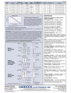
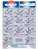
/
DOHVDQGRUSRUDWHIFH  Chicago Avenue Riverside California  Phone   Fax   SSOLFDWLRQVQJLQHHULQJ DOHVDQGRUSRUDWHIFH  Chicago Avenue Riverside California  Phone   Fax   SSOLFDWLRQVQJLQHHULQJ

DOHVDQGRUSRUDWHIFH Chicago Avenue Riverside California Phone Fax SSOLFDWLRQVQJLQHHULQJ - PDF document

stefany-barnette
stefany-barnette . @stefany-barnette
Follow
485 views
Uploaded On 2014-12-14

DOHVDQGRUSRUDWHIFH Chicago Avenue Riverside California Phone Fax SSOLFDWLRQVQJLQHHULQJ - PPT Presentation

Roseburg Oregon 974709422 Phone 541 4960700 Fax 541 4960408 H57360PDLO5737357347FDGGRFNFDGGRFN57361FRP573475747957347ZHE5737357347ZZZ57361FDGGRFN57361FRP For Caddock Distributors listed by country see caddockcomcontactdisthtml 2004 Caddock Electron ID: 23875

Roseburg Oregon 974709422 Phone

Share:

Link:

Embed:

Download Presentation from below link

Download Pdf The PPT/PDF document "DOHVDQGRUSRUDWHIFH Chicago Avenue River..." is the property of its rightful owner. Permission is granted to download and print the materials on this web site for personal, non-commercial use only, and to display it on your personal computer provided you do not modify the materials and that you retain all copyright notices contained in the materials. By downloading content from our website, you accept the terms of this agreement.


Presentation Transcript

Sales and Applications Engineering17271 North Umpqua Hwy. 28_IL134.0517 6 5 4 3 2 1 7 6 5 4 3 2 1 7 6 5 4 3 2 1 7 6 5 4 3 2 1 7 6 5 4 3 2 1 7 Input Voltage Dividers for Digital Multimeters and Range-Switching Instruments The exceptional performance of this extensive family of Type 1776 Precision Decade Resistor Voltage Dividers has There are now 39 standard models in the expanded family of Type 1776 precision resistor networks that include:For complete information on quantity price and delivery, contact our Sales Of�ce. 3, 4, and 5 - decade voltage dividers with ratios from 10:1 to 1,200 volts continuous ratings and overvoltage to 2,000 volts. Many combinations of Ratio and Absolute Tolerance, and Ratio and Absolute Temperature Coef�cient.combination of advantages provided by Caddock's Tetrinoxresistance �lms. This advanced film resistor technology provides the performance characteristics required by the precision input signal circuits of both bench-type In addition to requiring less board space, these compact precision resistor networks deliver higher performance than selected discrete resistor sets and thin-�lm networks.Schematic forType 1776 Precision Decade Resistor Voltage Dividers(Numbers inside circles reference columns in Model No. Ratio Tolerance: Maximum ratio error. (See the specific Figures for the Ratio De�nition).Ratio Temperature Coef�cient:Maximum ratio TC error. (See the specific Figures for the Ratio De�nition). Range 1: -40°C to +85°C.Range 2: 0°C to +70°C.Voltage Coefficient of Ratio R in series with any combination of R, R, R and 100 volts to rated voltage.Ratio stability of resistance under full load at +70°C, rated voltage applied to in series with any combination 6 5 4 3 2 1 7 6 5 4 3 2 1 7 % Change in Ratio 1776-C6112000.10.13010 ShelfLifeLoadLife 0.010.0050.01VoltageCoef.of Ratioppm/volt0.1RatioCppm/CAbs. TCCAbsoluteTolerance% VoltageRating R1R2R3R4R59 Meg 900 K 90 K 9 K 9006 1 2 3 4 5 6 7 1776-C61112000.10.0530100.010.0050.010.19 Meg900 K90 K9 K90061776-C6212000.10.130100.010.0050.010.19 Meg900 K90 K9 K1 K6 1776-C62112000.10.0530100.010.0050.010.19 Meg900 K90 K9 K1 K6 1776-C74212000.250.2550500.040.020.040.59 Meg900 K 1776-C7412000.10.150500.040.020.040.59 Meg900 K90 K9 K1 K7 1776-23212000.250.2550500.040.020.040.39 Meg900 K90 K9 K9003 1776-2312000.10.150500.020.010.020.29 Meg900 K90 K9 K9003 1776-24212000.250.2550500.040.020.040.39 Meg900 K90 K9 K1 K3 1776-2412000.250.150500.020.010.020.29 Meg900 K90 K9 K1 K3 1776-24112000.250.0550500.020.010.020.29 Meg900 K90 K9 K1 K3 1776-1051200+0, -0.50.13050.010.0050.010.029 Meg900 K90 K10 KN/A4 1776-C101200+0, -0.50.130100.010.0050.010.029 Meg900 K90 K10 KN/A9 1776-C1051200+0, -0.50.13050.010.0050.010.029 Meg900 K90 K10 KN/A9 1776-112000.250.0530100.010.0050.010.029 Meg900 K90 K10 KN/A2 1776-1412000.250.130100.010.0050.010.02 1776-812000.250.130250.020.010.020.29.9 Meg90 K10 KN/AN/A1 1776-912000.250.130100.010.0050.010.029.9 Meg90 K10 KN/AN/A1 1776-9112000.250.0530100.010.0050.010.029.9 Meg90 K10 KN/AN/A1 1776-91212000.250.023050.010.0050.010.029.9 Meg90 K10 KN/AN/A1 1776-C412000.250.2530100.010.0050.010.110 Meg1.1111M101.01K10.01K1.0001K8 1776-C4412000.10.130100.010.0050.010.110 Meg1.1111M101.01K10.01K1.0001K8 1776-C44112000.10.0530100.010.0050.010.110 Meg1.1111M101.01K10.01K1.0001K8 1776-C3412000.250.2550500.040.020.040.510 Meg1.1111M101.01K10.01K1.0001K8 1776-C5327500.250.2525250.020.010.020.4900 K90 K9 K900N/A5 1776-C537500.10.125150.020.010.020.3900 K90 K9 K900N/A5 1776-C5427500.250.2525250.02 1776-C547500.10.125150.020.010.020.3900 K90 K9 K1 KN/A5 1776-C5417500.10.0525150.020.010.020.3900 K90 K9 K1 KN/A5 1776-C621712000.10.0230100.010.0050.010.19 Meg900 K90 K9 K1 K6 Range 2Range 2Range 2Range 2Range 2Range 2Range 2Range 2Range 2Range 2Range 2Range 2Range 2Range 2Range 2Range 2Range 2Range 2Range 2Range 2Range 2Range 2Range 2Range 2Range 2Range 2Range 2Range 2Range 2Range 2TCp.Range 2 1776-C679 Meg900 K1776-C67112000.10.0530100.019 Meg900 K90 K9 K9001776-C671512000.13050.019 Meg900 K90 K9 K1776-C6812000.130100.019 Meg900 K90 K9 K1 K1776-C681512009 Meg900 K90 K9 K1 K1776-C4812000.10.11776-C48112001776-C68112000.130100.019 Meg900 K90 K9 K1 KRange 1Range 1Range 1Range 1Range 1Range 1Range 11776-C48151200Range 1 90010 Meg1.1111M101.01K10.01K1.0001K10 Meg = VOUT= VOUT= VOUT= VOUT1234 VIN10VIN VIN100VIN1,000VIN10,000 9K90K900K9M1K Page 1 of 2 © 2003-2017 Caddock Electronics, Inc. e-mail: caddock@caddock.com • web: www.caddock.com ELECTRONICS, INC. Sales and Applications Engineering17271 North Umpqua Hwy. RATIO DEFINITION: Where RRATIO 1 (RRATIO 2 (RRATIO 3 (RRATIO 4 (R .550 .020(13.97 .51) 1.600 .020(40.64 .51) .020 .002(.51 .05) .150 .040(3.81 1.02) .900 (22.86)1.100 (27.94)1.300 (33.02) 1.500 (38.10) .700 (17.78) .010 .002(.26 .05) CADDOCK1203 1776-C74 .100(2.54) MAX.PIN 1.050(1.27) .550 .020(13.97 .51) 1.500 .020(38.10 .51) .020 .002(.51 .05) .150 .040(3.81 1.02) .900 (22.86)1.100 (27.94)1.200 (30.48) 1.300 (33.02) .700 (17.78) .010 .002(.26 .05) CADDOCK0620 1776-C34 1.400 (35.56) .100(2.54) MAX.PIN 1.050(1.27) .600 .020(15.24 .51) 1.600 .020(40.64 .51) .020 .002(.51 .05) .150 .040(3.81 1.02) .800 (20.32)1.000 (25.40)1.100 (27.94) 1.300 (33.02) .700 (17.78) .010 .002(.26 .05) CADDOCK0605 1776-C10 1.400 (35.56) 1.500 (38.10) .100(2.54) MAX.PIN 1.050(1.27) 1.200 .020(30.48 .51) .550 .020(13.97 .51).100(2.54) MAX. CADDOCK0417 1776-C54 .020 .002(.51 .05) .150 .040(3.81 1.02) .800 (20.32).900 (22.86)1.100 (27.94) .600 (15.24) .010 .002(.26 .05) PIN 1.050(1.27) 1.700 .020(43.18 .51) .750 .020(19.05 .51) CADDOCK ELECTRONICSMODEL 1776-C105 1202 .250 .050(6.35 1.27) .800 (20.32)1.000 (25.40)1.100 (27.94) 1.300 (33.02) 1.400 (35.56) 1.500 (38.10) .700 (17.78) .090(2.29) MAX..025 .002(.64 .05) DIA.Tinned CopperPIN 1.100(2.54) 2.000 .020(50.80 .51) .680 .020(17.27 .51) .250 .050(6.35 1.27) 1.000 (25.40)1.200 (30.48)1.500 (38.10) 1.800 (45.72) .800 (20.32)CADDOCK ELECTRONICSMODEL 1776-23 0619 .090(2.29) MAX..025 .002(.64 .05) DIA.Tinned CopperPIN 1.1002.54) .750 .020(19.05 .51) 1.700 .020(43.18 .51) CADDOCK ELECTRONICSMODEL 1776-1 0604 .250 .050(6.35 1.27) 1.200 (30.48)1.400 (35.56)1.500 (38.10) .900 (22.86) .090(2.29) MAX..025 .002(.64 .05) DIA.Tinned CopperPIN 1.1002.54) .680 .020(17.27 .51) 1.500 .020(38.10 .51) .090(2.29) MAX. .025 .002(.64 .05) DIA.Tinned Copper PIN 1.250 .050(6.35 1.27) .100(2.54) 1.100 (27.94)1.300 (33.02) .900 (22.86) CADDOCK ELECTRONICSMODEL 1776-8 1225 R1R2R3R4 123 45 R1R2 123 R3R4 45 R5 6 R1R2R3R4 123 45 123 4 R1R2R3 R 1 R 2 1234 R 3 R 4 5678 R1R2 124 R3R456 R573 R1R2 123 R3R4 45 R5 6 R1R2 1234 R3R4 5678 R 1 R 2 123 R 3 R 4 45 R 5 6 RATIO DEFINITION:RATIO 1RATIO 2RATIO 3RATIO 4RATIO DEFINITION:ALL RESISTORS RATIO RATIO DEFINITION:ALL RESISTORS RATIO RATIO DEFINITION:ALL RESISTORS RATIO RATIO DEFINITION:ALL RESISTORS RATIO RATIO DEFINITION:ALL RESISTORS RATIO RATIO DEFINITION:ALL RESISTORS RATIO RATIO DEFINITION:ALL RESISTORS RATIO DIMENSIONS IN INCHES AND (MILLIMETERS) .550 .020(13.97 .51) 1.400 .020(35.56 .51) .020 .002(.51 .05) .150 .040(3.81 1.02) .900 (22.86)1.000 (25.40)1.100 (27.94) 1.300 (33.02) .700 (17.78) CADDOCK0611 1776-C62 .010 .002(.26 .05) .100(2.54) MAX.PIN 1.050(1.27) Figure 11 Lead Form Detail Note: Lead R1R2 123 R3R4 45 R5 6 R1R2 124 R3R456 R573 RATIO DEFINITION: Where RRATIO 1 (RRATIO 2 (RRATIO 3 (RRATIO 4 (RRATIO DEFINITION:RATIO 1RATIO 2RATIO 3RATIO 4 1.000 .020 (25.40 .51) .050(1.27) 0.530 .020(13.46 .51) 0.020 .002(0.51 .05).500 (12.70) 0.110(2.79) Max. 0.010 .002(0.25 .05).600 (15.24) .700 (17.78).800 (20.32) .900 (22.86)See Lead Form Detail Note..150 .040(3.81 1.02) CADDOCK0617 1776-C68 PIN 1 1.200 .020 (30.48 .51) .050(1.27) 0.530 .020(13.46 .51) 0.020 .002(0.51 .05).500 (12.70) 0.110(2.79) Max. 0.010 .002(0.25 .05).700 (17.78) .800 (20.32).900 (22.86)1.000 (25.40)1.100 (27.94)See Lead Form Detail Note..150 .040(3.81 1.02) CADDOCK0617 1776-C48 PIN 1  New Smaller Models at Lower CostPage 2 of 2 © 2003-2017 Caddock Electronics, Inc. e-mail: caddock@caddock.com • web: www.caddock.com ELECTRONICS, INC. © 2003-2017 Caddock Electronics, Inc. e-mail: caddock@caddock.com • web: www.caddock.com ELECTRONICS, INC. © 2003-2017 Caddock Electronics, Inc. e-mail: caddock@caddock.com • web: www.caddock.com ELECTRONICS, INC. 28_IL Sales and Applications Engineering17271 North Umpqua Hwy. RATIO DEFINITION: Where RRATIO 1 (RRATIO 2 (RRATIO 3 (RRATIO 4 (R .550 .020(13.97 .51) 1.600 .020(40.64 .51) .020 .002(.51 .05) .150 .040(3.81 1.02) .900 (22.86)1.100 (27.94)1.300 (33.02) 1.500 (38.10) .700 (17.78) .010 .002(.26 .05) CADDOCK1203 1776-C74 .100 (2.54) MAX.PIN 1.050(1.27) .550 .020(13.97 .51) 1.500 .020(38.10 .51) .020 .002(.51 .05) .150 .040(3.81 1.02) .900 (22.86)1.100 (27.94)1.200 (30.48) 1.300 (33.02) .700 (17.78) .010 .002(.26 .05) CADDOCK0620 1776-C34 1.400 (35.56) .100 (2.54) MAX.PIN 1.050(1.27) .600 .020(15.24 .51) 1.600 .020(40.64 .51) .020 .002(.51 .05) .150 .040(3.81 1.02) .800 (20.32)1.000 (25.40)1.100 (27.94) 1.300 (33.02) .700 (17.78) .010 .002(.26 .05) CADDOCK0605 1776-C10 1.400 (35.56) 1.500 (38.10) .100 (2.54) MAX.PIN 1.050(1.27) 1.200 .020(30.48 .51) .550 .020(13.97 .51).100 (2.54) MAX. CADDOCK0417 1776-C54 .020 .002(.51 .05) .150 .040(3.81 1.02) .800 (20.32).900 (22.86)1.100 (27.94) .600 (15.24) .010 .002(.26 .05) PIN 1.050(1.27) 1.700 .020(43.18 .51) .750 .020(19.05 .51) CADDOCK ELECTRONICSMODEL 1776-C105 1202 .250 .050(6.35 1.27) .800 (20.32)1.000 (25.40)1.100 (27.94) 1.300 (33.02) 1.400 (35.56) 1.500 (38.10) .700 (17.78) .090 (2.29) MAX..025 .002(.64 .05) DIA.Tinned CopperPIN 1.100(2.54) 2.000 .020(50.80 .51) .680 .020(17.27 .51) .250 .050(6.35 1.27) 1.000 (25.40)1.200 (30.48)1.500 (38.10) 1.800 (45.72) .800 (20.32)CADDOCK ELECTRONICSMODEL 1776-23 0619 .090 (2.29) MAX..025 .002(.64 .05) DIA.Tinned CopperPIN 1.100(2.54) .750 .020(19.05 .51) 1.700 .020(43.18 .51) CADDOCK ELECTRONICSMODEL 1776-1 0604 .250 .050(6.35 1.27) 1.200 (30.48)1.400 (35.56)1.500 (38.10) .900 (22.86) .090 (2.29) MAX..025 .002(.64 .05) DIA.Tinned CopperPIN 1.100(2.54) .680 .020(17.27 .51) 1.500 .020(38.10 .51) .090 (2.29) MAX. .025 .002(.64 .05) DIA.Tinned Copper PIN 1.250 .050(6.35 1.27) .100(2.54) 1.100 (27.94)1.300 (33.02) .900 (22.86) CADDOCK ELECTRONICSMODEL 1776-8 1225 R1R2R3R4 123 45 R1R2 123 R3R4 45 R5 6 R1R2R3R4 123 45 123 4 R1R2R3 R 1 R 2 1234 R 3 R 4 5678 R1R2 124 56 R573 R1R2 123 R3R4 45 R5 6 R1R2 1234 R3R4 5678 R 1 R 2 123 R 3 R 4 45 R 5 6 RATIO DEFINITION:RATIO 1 RATIO 2 RATIO 3 RATIO 4 RATIO DEFINITION:ALL RESISTORS RATIO ALL RESISTORS RATIO ALL RESISTORS RATIO ALL RESISTORS RATIO ALL RESISTORS RATIO ALL RESISTORS RATIO ALL RESISTORS RATIO ONE ANOTHERDIMENSIONS IN INCHES AND (MILLIMETERS) .550 .020(13.97 .51) 1.400 .020(35.56 .51) .020 .002(.51 .05) .150 .040(3.81 1.02) .900 (22.86)1.000 (25.40)1.100 (27.94) 1.300 (33.02) .700 (17.78) CADDOCK0611 1776-C62 .010 .002(.26 .05) .100 (2.54) MAX.PIN 1.050(1.27) Figure 11 Lead Form Detail Note: Lead form detail provides interference R1R2 123 R3R4 45 R5 6 R1R2 124 56 R573 RATIO DEFINITION: Where RRATIO 1 (RRATIO 2 (RRATIO 3 (RRATIO 4 (RRATIO DEFINITION:RATIO 1 RATIO 2 RATIO 3 RATIO 4 R1:R5 1.000 .020 (25.40 .51) .050(1.27) 0.530 .020(13.46 .51) 0.020 .002(0.51 .05).500 (12.70) 0.110(2.79) Max. 0.010 .002(0.25 .05).600 (15.24) .700 (17.78).800 (20.32) .900 (22.86)See Lead Form Detail Note..150 .040(3.81 1.02) CADDOCK0617 1776-C68 PIN 1 1.200 .020 (30.48 .51) .050(1.27) 0.530 .020(13.46 .51) 0.020 .002(0.51 .05).500 (12.70) 0.110(2.79) Max. 0.010 .002(0.25 .05).700 (17.78) .800 (20.32).900 (22.86)1.000 (25.40)1.100 (27.94)See Lead Form Detail Note..150 .040(3.81 1.02) CADDOCK0617 1776-C48 PIN 1  New Smaller Models at Lower CostPage 2 of 2 Sales and Applications Engineering17271 North Umpqua Hwy. 28_IL 6 5 4 3 2 1 7 6 5 4 3 2 1 7 6 5 4 3 2 1 7 6 5 4 3 2 1 7 6 5 4 3 2 1 7 Input Voltage Dividers for Digital Multimeters and Range-Switching Instruments The exceptional performance of this extensive family of Type 1776 Precision Decade Resistor Voltage Dividers has There are now 39 standard models in the expanded family of Type 1776 precision resistor networks that include:For complete information on quantity price and delivery, contact our Sales Of�ce.3, 4, and 5 - decade voltagedividers with ratios from 10:1 to1,200 volts continuous ratingsand overvoltage to 2,000 volts.Many combinations of Ratio andAbsolute Tolerance, and Ratioand Absolute Temperaturecombination of advantages provided by Caddock's Tetrinoxresistance �lms. This advanced film resistor technology provides the performance characteristics required by the precision input signal circuits of both bench-type In addition to requiring less board space, these compact precision resistor networks deliver higher performance than selected discrete resistor sets and thin-�lm networks.Schematic forType 1776 Precision Decade Resistor Voltage Dividers(Numbers inside circles reference columns in Model No. Ratio Tolerance: Maximum ratio error. (See the specific Figures for the Ratio De�nition).Ratio Temperature Coef�cient:Maximum ratio TC error. (See the specific Figures for the Ratio De�nition). Range 1: -40°C to +85°C.Range 2: 0°C to +70°C.Voltage Coefficient of Ratio R in series with any combination of R, R, R and 100 volts to rated voltage.Ratio stability of resistance under full load at +70°C, rated voltage applied to in series with any combination Shelf Stability of Ratio: Six Overvoltage: Maximum voltage of 1.67 times rated DC voltage. Volts DC or peak AC applied to R and any combination of R, R, R and for 10 Voltage Rating: DC or RMS AC voltage applied to R in series with any combination of and RStorage Temperature: -40°C 6 5 4 3 2 1 7 6 5 4 3 2 1 7 % Change in Ratio 12000.1 ShelfLifeLoadLife 0.010.0050.01VoltageCoef.of Ratioppm/volt0.1RatioTCppm/CAbs. TCppm/CAbsoluteTolerance% VoltageRating R1R2R3R4R59 Meg 900 K 90 K 9 K 9006 1 2 3 4 5 6 7 301090 K9 K9006301090 K9 K1 K6 301090 K9 K1 K6 505090 K9 K1 K7 505090 K9 K1 K7 505090 K9 K9003 505090 K9 K9003 505090 K9 K1 K3 505090 K9 K1 K3 505090 K9 K1 K3 30590 K10 KN/A4 301090 K10 KN/A9 30590 K10 KN/A9 301090 K10 KN/A2 301090 K10 KN/A2 302510 KN/AN/A1 301010 KN/AN/A1 301010 KN/AN/A1 30510 KN/AN/A1 3010101.01K10.01K1.0001K8 3010101.01K10.01K1.0001K8 3010101.01K10.01K1.0001K8 5050101.01K10.01K1.0001K8 25259 K900N/A5 25159 K900N/A5 25259 K1 KN/A5 25159 K1 KN/A5 25159 K1 KN/A5 301090 K9 K1 K6 Range 2Range 2Range 2Range 2Range 2Range 2Range 2Range 2Range 2Range 2Range 2Range 2Range 2Range 2Range 2Range 2Range 2Range 2Range 2Range 2Range 2Range 2Range 2Range 2Range 2Range 2Range 2Range 2Range 2Range 2TCTemp.Range 2 301090 K9 K90030590 K9 K301090 K9 K1 K90 K9 K1 K301090 K9 K1 K 101.01K10.01K1.0001K101.01K10.01K1.0001K101.01K10.01K1.0001K12000.190 K9 K900 = VOUT= VOUT= VOUT= VOUT1234 VIN10VIN VIN100VIN1,000VIN10,000 9K90K900K9M1K Page 1 of 2