/
TC fd Hz th Order Butterworth Lowpass Filter Filter Amplitude Response and Noise Lowpass TC fd Hz th Order Butterworth Lowpass Filter Filter Amplitude Response and Noise Lowpass

TC fd Hz th Order Butterworth Lowpass Filter Filter Amplitude Response and Noise Lowpass - PDF document

stefany-barnette
stefany-barnette . @stefany-barnette
Follow
582 views
Uploaded On 2014-12-17

TC fd Hz th Order Butterworth Lowpass Filter Filter Amplitude Response and Noise Lowpass - PPT Presentation

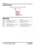
Its unusual architecture puts the filter outside the DC path so DC offset and low frequency noise problems are eliminated This makes the LTC1062 very useful for lowpass filters where DC accuracy is important The filter input and output are simultane ID: 25452

Its unusual architecture puts

Share:

Link:

Embed:

Download Presentation from below link

Download Pdf The PPT/PDF document "TC fd Hz th Order Butterworth Lowpass Fi..." is the property of its rightful owner. Permission is granted to download and print the materials on this web site for personal, non-commercial use only, and to display it on your personal computer provided you do not modify the materials and that you retain all copyright notices contained in the materials. By downloading content from our website, you accept the terms of this agreement.


Presentation Transcript

1L 10Hz 5th Order Butterworth Lowpass FilterFilter Amplitude Response and Noise RATIO = Ð5VDC ACCURATENOTE: TO ADJUST OSCILLATOR FREQUENCY,USE A 6800pF CAPACITOR IN SERIES Ð80Ð60Ð40Ð2010100 Ð90Ð50 OSC = 3900pF FEATURESAPPLICATIO STYPICAL APPLICATIO , LTC and LT are registered trademarks of Linear Technology Corporation. 5th Order Lowpass Filter 3L = Ð5V, unless otherwise specified, AC output measured at Pin 7, PARAMETERCONDITIONSMINTYPMAXUNITS Internal Buffer 250pA1701000pA 220mV Voltage SwingR3.8V 40/3mA Clock (Note 3) Internal Oscillator FrequencyC, Pin 11 in SW16) = 100pF253250kHz1565kHz Max Clock Frequency4MHz 4080 Absolute Maximum Ratings are those values beyond which the life of is the frequency where the gain is Ð3dB with respect to the inputThe external or driven clock frequency is divided by either 1, 2 or 4depending upon the voltage at Pin 4. For the N8 package, when Pin 4 = VÐ80Ð60Ð40Ð20110 Ð90Ð70Ð50Ð30 2RC=VS = ±2.5VTA = 25°C fC1.62 CLK = 500kHz, fC = 5kHz CLK = 250kHz, fC = 2.5kHz CLK = 100kHz, fC = 1kHz CLK = 1kHz, fC = 10Hz Ð80Ð60Ð40Ð20110 Ð90Ð70Ð50Ð30 2RC=VS = ±2.5VTA = 25°C fC1.62 CLK = 500kHz, fC = 5kHz CLK = 250kHz, fC = 2.5kHz CLK = 100kHz, fC = 1kHz CLK = 1kHz, fC = 10Hz CLK = 10kHz, fC = 100HzfIN/fCÐ1.0Ð0.4Ð0.6Ð0.80.40.20Ð0.21062 G03 0.10.20.40.60.8 S = ±5VTA = 25°CfCLK = 100kHz 2RC= fC1.6 2RC= fC1.62 2RC= fC1.64 Amplitude Response Normalizedto the Cutoff FrequencyPassband Gainvs Input FrequencyELECTRICAL CHARACTERISTICS TYPICAL PERFOR A CE CHARACTERISTICS 4L vs Input FrequencyFilter Noise Spectral Density 0.10.20.40.60.8 S = ±5VfCLK = 100kHz12RC= fC1.62 A = 125°C = Ð55 fIN/fCÐ210Ð120Ð1500Ð30Ð90 0.10.20.40.60.8 S = ±5Vf12RC= fC1.62 TA = 25°C 0.11010010k 101 1k60400 S = ±5VTA = 25°C C = 10Hz C = 1kHz C = 100Hz Normalized Oscillator Frequency,f vs Supply VoltageOscillator Frequency, fOSCvs Ambient TemperatureV4OSCILLATOR FREQUENCY NORMALIZEDTO fOSC AT 5V SUPPLY1.11.2201062 G07 1.00.90.7812161861014 0.81.61.5 Ð50Ð25 + = 10VVÐ = 0V + = 5VVÐ = 0V Power Supply Currentvs Power Supply VoltagePOWER SUPPLY VOLTAGE (V)4SUPPLY CURRENT (mA)812201062 G09 40812166101418 16610214 = Ð55 A = 25°C A = 125°C TYPICAL PERFOR A CE CHARACTERISTICS 6L maximum attenuation is due to the rolloff at higherquency, the maximum attenuation is about 64dB. A 4kHz,maximum flat filter would have dictated. The LTC1062RMS noise from DC to 17kHz was 100Pin5 is floating, an internal 33pF capacitor plus thePin5 can also be driven with an external CMOS clock toage levels and more than enough output current to VV 2.5V0.9VÐ1V 5V1.3VÐ2.1V 6V1.7VÐ2.5V 7V1.75VÐ2.9V 110 6Ð12 2RC= fC1.62 VS = ±5VFigure 2. Amplitude Response of Pin 1Internal BufferThe internal buffer out (Pin 8) and Pin 1 are part of thesignal AC path. Excessive capacitive loading will causegain errors in the passband, especially around the cutofffrequency. The internal buffer gain at DC is typically0.006dB. The internal buffer output can be used as a filteroutput, however, it has a few millivolts of DC offset. Thetemperature coefficient of the internal buffer is typically1µV/°C.Filter AttenuationThe LTC1062 rolloff is typically 30dB/octave. When theclock and the cutoff frequencies increase, the filterÕsmaximum attenuation decreases. This is shown in the APPLICATIO S I FOR ATIO 8L from a Single Positive Supply, V RATIO1062 TA03 VINV+100kVOUTVÐ Adding an External (R1, C1) to Eliminate the Clock Feedthrough andto Improve the High Frequency Attenuation Floor RATIO1062 TA04 C10.01CVINRVÐ 10R +BUFFER RATIO1062 TA05 C0.01µF = Ð5V = 1kHz. THE FILTER ACCURATELY PASSESTHE HIGH DC INPUT AND ACTS AS 5TH ORDER LP FILTER 0.11 0.2Ð1.2Ð0.80Ð0.4 S = ±5VfCLK = 100kHz TYPICAL APPLICATIO S 10 Simple Cascading Technique RATIODC ACCURATE1062 TA11 10Hz, 10TH ORDER DC ACCURATE LOWPASS FILTER60dB/OCTAVE ROLLOFF0.5dB PASSBAND ERROR, 0dB DC GAINMAXIMUM ATTENUATION110dB (fÐ5VÐ5V RATIO Ð5V +TC1052100Hz, 50Hz, 25Hz 5th Order DC Accurate LP Filter RATIO1062 TA12 0.1µF1234 Ð5V5V µFVOUT BY CONNECTING PIN 4 OF THE LTC1062HIGH/GROUND/LOW THE FILTER CUTOFFÐ5VÐ5V 100k 100k TYPICAL APPLICATIO S 12 RATIO1062 TA15 20kR320kR410k + 19.35k R510k 1/2 LT1013 1/2 LT1013 R720kC70.1µF 2RC= fCLK100 ¥ 1.62 101001k TYPICAL APPLICATIO S 14 N8 Package8-Lead PDIP (Narrow .300 Inch)(Reference LTC DWG # 05-08-1510) N8 1002 (1.651)TYP .045 Ð .065(1.143 Ð 1.651) .130 ± .005(3.302 ± 0.127) .020(0.508)MIN .018 ± .003(0.457 ± 0.076) .120(3.048)MIN 4 876 .400*(10.160)MAX (0.203 Ð 0.381) (7.620 Ð 8.255) .325+.035Ð.015+0.889Ð0.3818.255 1. DIMENSIONS AREINCHESMILLIMETERS*THESE DIMENSIONS DO NOT INCLUDE MOLD FLASH OR PROTRUSIONS. MOLD FLASH OR PROTRUSIONS SHALL NOT EXCEED .010 INCH (0.254mm) .100(2.54)BSCU 16 INEAR TECHNOLOGY CORPORATION 1994Linear Technology Corporation630 McCarthy Blvd., Milpitas, CA 95035-7417(408) 432-1900 FAX: (408) 434-0507 RATIO1062 TA17Ð5V + + TYPICAL APPLICATIO PART NUMBERDESCRIPTIONCOMMENTS LTC10635th Order Butterworth Lowpass, DC AccurateClock Tunable, No External Components LTC10655th Order Bessel Lowpass, DC AccurateClock Tunable, No External Components LTC1066-18th Order Elliptic or Linear Phase, DC AccurateClock Tunable, fc LTC1563-3Active RC, 4th Order LowpassVery Low Noise, 256Hz LTC156410kHz to 150kHz Digitally Controlled Lowpass and PGAContinuous Time, Very High Dynamic Range, PGA Included LTC1569-6Linear Phase, DC Accurate, 10th OrderNo External Clock Required, fc LTC1569-7Linear Phase, DC Accurate, 10th OrderNo External Clock Required, fc RELATED PARTS