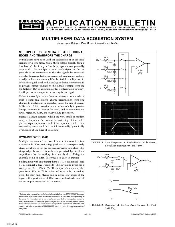
PDF-FIGURE 3. An Input Current Flows Through the Protection Diodes and RF.

Author : tatyana-admore | Published Date : 2016-06-29

RF 10kW C1 100nF100nF R1 10kW10kW VC 110 IN F 10kW 0V VOUT VINIt VINt

Presentation Embed Code

Download Presentation

Download Presentation The PPT/PDF document "FIGURE 3. An Input Current Flows Through..." is the property of its rightful owner. Permission is granted to download and print the materials on this website for personal, non-commercial use only, and to display it on your personal computer provided you do not modify the materials and that you retain all copyright notices contained in the materials. By downloading content from our website, you accept the terms of this agreement.

FIGURE 3. An Input Current Flows Through the Protection Diodes and RF.: Transcript


RF 10kW C1 100nF100nF R1 10kW10kW VC 110 IN F 10kW 0V VOUT VINIt VINt. In practice there are always two input bias currents I B and I B see Figure 1 Rev0 1008 WK Page 1 of 5 A very variable parameter B can vary from 60 fA 1 electron every 3 s to many A depending on the device Some structures have wellmatched I others In practice there are always two input bias currents I B and I B see Figure 1 Rev0 1008 WK Page 1 of 5 A very variable parameter B can vary from 60 fA 1 electron every 3 s to many A depending on the device Some structures have wellmatched I others Course . Code : . 11-EC201. DEPARTMENT . OF . ELECTRONICS & COMPUTER . ENGINEERING. The . two modes of operation of ideal diodes and the use of an external circuit to limit the forward current (a) and the reverse voltage (b).. Keith Weaver. James . Mulford. Philip Estrada. What . is digital to analog converter (DAC)?. Types . of DAC. Binary Weighted Resistor. R-2R Ladder. Discuss Specifications:. Reference Voltages. Resolution. Lecture. 3. 1. Discrete Semiconductor Devices. Semiconductor Materials. Conductor and Insulators.. N-type, P-Type, electron, and hole current. PN junction, depletion region, potential barrier.. Diodes. Course . Code : . 11-EC201. DEPARTMENT . OF . ELECTRONICS & COMPUTER . ENGINEERING. Diodes. Contents . Introduction, . Ideal Diode, . Physical Operation of PN Junction Diode,. Terminal Characteristics of Junction Diodes,. Silicon Semiconductors. Doped Semiconductors. P-N Junction. Extra holes combine with extra electrons to form depletion zone. Forward Bias. Diode conducts only when it is . forward-biased. .. Reverse Bias. Bill Leonard N0CU. 7 April 2018. Topics. What damages receiver front ends. Common types of receiver front end protectors. Example: homebrew protector. What Damages Receiver Front Ends?. Damage results from exceeding a semiconductor’s junction breakdown voltage. Center for Mobile Hands-On STEM. SMART LIGHTING Engineering Research Center. ECSE Department. Rensselaer Polytechnic Institute. Intro to ECSE Analysis. Outline. Diodes – What is their basic function?. Logan J Lauder. Background . 6.5 million E.Vs on the road today. Typically operating between 12V – 400V. DC or AC current . Overview . IGBTs for inverters and motor controllers. Fast switching power MOSFETS . GUIDED BY. Mr.m.v.patil. SUBMITTED BY. Nivedita Dattatray Sabale (117141). Bhagyashri dhudaku Bhadange (117107). Sonali narendra walekar (127183). Shital Santosh Ahire (117103). Assistant Professor. Department of Electronics. St. Joseph’s College, . Trichy. . . What Are Diodes Made Out Of?. Silicon (Si) and Germanium (Ge) are the two most common single elements that are used to make Diodes. A compound that is commonly used is Gallium Arsenide (GaAs), especially in the case of LEDs because of it’s large bandgap. . A . pn. junction is known as a . semi-conductor . or . crystal . diode. .. The outstanding property of a crystal diode to conduct current in . one direction . only permits it to be used as a rectifier. Presented By Prof. D. M. Parshuramkar. N-Type Material. N-Type Material:. When extra valence electrons are introduced into a material such as silicon an n-type material is produced. The extra valence electrons are introduced by putting impurities or .

Download Document

Here is the link to download the presentation.
"FIGURE 3. An Input Current Flows Through the Protection Diodes and RF."The content belongs to its owner. You may download and print it for personal use, without modification, and keep all copyright notices. By downloading, you agree to these terms.

Related Documents