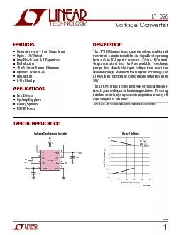
/
LT fb Voltage Converter The LT  is a switched capacitor voltage doubler and inverter on LT fb Voltage Converter The LT  is a switched capacitor voltage doubler and inverter on

LT fb Voltage Converter The LT is a switched capacitor voltage doubler and inverter on - PDF document

tawny-fly
tawny-fly . @tawny-fly
Follow
641 views
Uploaded On 2014-12-22

LT fb Voltage Converter The LT is a switched capacitor voltage doubler and inverter on - PPT Presentation

Capable of operating from a 4V to 10V input it provides 7V to 18V output Output currents of over 10mA are available Two charge pumps first double the input voltage then invert the doubled voltage Manufactured in bipolar technology the LT1026 is not ID: 27719

Capable operating from

Share:

Link:

Embed:

Download Presentation from below link

Download Pdf The PPT/PDF document "LT fb Voltage Converter The LT is a swi..." is the property of its rightful owner. Permission is granted to download and print the materials on this web site for personal, non-commercial use only, and to display it on your personal computer provided you do not modify the materials and that you retain all copyright notices contained in the materials. By downloading content from our website, you accept the terms of this agreement.


Presentation Transcript

LT1026 Ð10 Ð10 µFVIN = 5VTA = 25¡C L = 0 Ð10 µFVIN = 5VTA = 25¡C L = 0 Supply CurrentSupply Current5101520 5101520 µFVIN = 5VTA = 25¡CNEGATIVE 5101520 µFVIN = 5VTA = 25¡CPOSITIVE PARAMETERSCONDITIONSMINTYPMAXUNITS Supply CurrentV = 4VI712.5mA = 10VI1530mA Absolute Maximum Ratings are those values beyond which the life of min = Ð4.5 for T LT1026 NSStandard Configuration Voltage Doubler and InverterVoltage Quadrupler LT1026 1µFVIN + +VOUTµFÐVOUT + 1026 ¥ TA05 LT1026 + 1µF (FLOATING) + +VOUTµFC21µF 1026 ¥ TA06 Parallel Converters for Higher Output Current and Lower Output Impedance LT1026 + 1µFVIN 1µF LT1026 + 1µFVIN 1µF 1026 ¥ TA07 +VµF µFÐVPositive to Negative Converter LT1026 + ÐVOUTµF 1026 ¥ TA03 LT1026 + µFVIN µF 1026 ¥ TA04 LT1026 Information furnished by Linear Technology Corporation is believed to be accurate and reliable.However, no responsibility is assumed for its use. Linear Technology Corporation makes no represen-tation that the interconnection of its circuits as described herein will not infringe on existing patent rights.PACKAGE DESCRIPTIONN8 Package8-Lead PDIP (Narrow .300 Inch)(Reference LTC DWG # 05-08-1510)S8 Package8-Lead Plastic Small Outline (Narrow 0.150)(LTC DWG # 05-08-1610)N8 1002 (1.651)TYP .045 Ð .065(1.143 Ð 1.651) .130 ± .005(3.302 ± 0.127) .020(0.508)MIN .018 ± .003(0.457 ± 0.076) .120(3.048)MIN (0.203 Ð 0.381) (7.620 Ð 8.255) +0.889Ð0.381 34 876 .400*(10.160)MAX NOTE:1. DIMENSIONS AREINCHESMILLIMETERS*THESE DIMENSIONS DO NOT INCLUDE MOLD FLASH OR PROTRUSIONS. MOLD FLASH OR PROTRUSIONS SHALL NOT EXCEED .010 INCH (0.254mm) .100(2.54)BSC (0.406 Ð 1.270) .010 Ð .020(0.254 Ð 0.508)´ 45°0¡Ð 8¡ TYP.008 Ð .010(0.203 Ð 0.254) (1.346 Ð 1.752) .014 Ð .019(0.355 Ð 0.483)TYP .004 Ð .010(0.101 Ð 0.254) .050(1.270)BSC 234 .150 Ð .157(3.810 Ð 3.988)NOTE 3 8765 .189 Ð .197(4.801 Ð 5.004)NOTE 3 .228 Ð .244(5.791 Ð 6.197) RECOMMENDED SOLDER PAD LAYOUT .045 ±.005 .050 BSC.030 ±.005 TYP INCHES(MILLIMETERS)NOTE:1. DIMENSIONS IN 2. DRAWING NOT TO SCALE3. THESE DIMENSIONS DO NOT INCLUDE MOLD FLASH OR PROTRUSIONS.J8 Package8-Lead CERDIP (Narrow .300 Inch, Hermetic)(Reference LTC DWG # 05-08-1110)J8 0801 .014 Ð .026(0.360 Ð 0.660) .200(5.080)MAX .015 Ð .060(0.381 Ð 1.524).1253.175MIN .100(2.54)BSC (7.62 BSC).008 Ð .018(0.203 Ð 0.457) 0¡ Ð 15¡ (0.127)MIN.405(10.287)MAX.220 Ð .310(5.588 Ð 7.874) 34 (0.635)RAD TYP .045 Ð .068(1.143 Ð 1.650)FULL LEADOPTION .023 Ð .045(0.584 Ð 1.143)HALF LEADOPTION (4 PLCS) .045 Ð .065(1.143 Ð 1.651) OBSOLETE PACKAGE