PDF-VOLTAGE REFERENCEFEATURESOUTPUT VOLTAGE: +5V C to +85 max (0.1Hz to 10
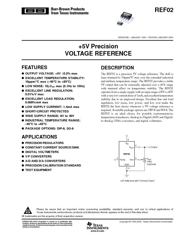
VREF02Trim
654
ROutput
EF02
SBVS003B
Download Presentation
"VOLTAGE REFERENCEFEATURESOUTPUT VOLTAGE: +5V C to +85 max (0 " is the property of its rightful owner. Permission is granted to download and print materials on this website for personal, non-commercial use only, provided you retain all copyright notices. By downloading content from our website, you accept the terms of this agreement.
Presentation Transcript
Transcript not available.