/
APPLICATION BULLETIN Mailing Address PO Box   Tucson AZ   Street Address  S APPLICATION BULLETIN Mailing Address PO Box   Tucson AZ   Street Address  S

APPLICATION BULLETIN Mailing Address PO Box Tucson AZ Street Address S - PDF document

test
test . @test
Follow
502 views
Uploaded On 2014-12-12

APPLICATION BULLETIN Mailing Address PO Box Tucson AZ Street Address S - PPT Presentation

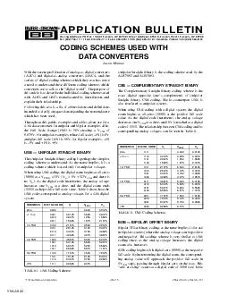
Tucson Blvd Tucson AZ 85706 Tel 602 7461111 Twx 910952111 Telex 0666491 FAX 602 8891510 Immediate Product Info 800 5486132 TABLE I USB Coding Scheme MNEMONIC DIGITAL CODE V t CODE t Zero 0000 0000 03125 1 V LSB 0001 03125 0625 09375 0010 09375 ID: 22954

Tucson Blvd Tucson

Share:

Link:

Embed:

Download Presentation from below link

Download Pdf The PPT/PDF document "APPLICATION BULLETIN Mailing Address PO ..." is the property of its rightful owner. Permission is granted to download and print the materials on this web site for personal, non-commercial use only, and to display it on your personal computer provided you do not modify the materials and that you retain all copyright notices contained in the materials. By downloading content from our website, you accept the terms of this agreement.


Presentation Transcript

APPLICATION BULLETIN ¨ MNEMONICDIGITAL CODEVZero00000.0000.312500010.31250.6250.937500100.93751.2501.562500111.56251.8752.18751/4 FSR01002.18752.5002.812501012.81253.1253.437501103.43753.7504.062501114.06254.3754.68751/2 FSR10004.68755.0005.312510015.31255.6255.937510105.93756.2506.562510116.56256.8757.18753/4 FSR11007.18757.5007.812511017.81258.1258.437511108.43758.7509.0625+FS11119.06259.375 MNEMONICDIGITAL CODEVZero11110.0000.312511100.31250.6250.937511010.93751.2501.562511001.56251.8752.18751/4 FSR10112.18752.5002.812510102.81253.1253.437510013.43753.7504.062510004.06254.3754.68751/2 FSR01114.68755.0005.312501105.31255.6255.937501015.93756.2506.562501006.56256.8757.18753/4 FSR00117.18757.5007.812500107.81258.1258.437500018.43758.7509.0625+FS00009.06259.375 steps, passing through bipolar zero on the way. This DATA CONVERTERS MNEMONICDIGITAL CODEVÐFS0000Ð5.000Ð4.68750001Ð4.6875Ð4.375Ð4.06250010Ð4.0625Ð3.750Ð3.43750011Ð3.4375Ð3.125Ð2.81251/2 ÐFS0100Ð2.8125Ð2.500Ð2.18750101Ð2.1875Ð1.875Ð1.56250110Ð1.5625Ð1.250Ð0.93750111Ð0.9375Ð0.625Ð0.3125BPZ1000Ð0.31250.000+0.31251001+0.3125+0.625+0.93751010+0.9375+1.250+1.56251011+1.5625+1.875+2.18751/2 +FS1100+2.1875+2.500+2.81251101+2.8125+3.125+3.43751110+3.4375+3.750+4.0625+FS1111+4.0625+4.375 steps, passing through bipolar zero on the way.MNEMONICDIGITAL CODEVÐFS1111Ð5.000Ð4.68751110Ð4.6875Ð4.375Ð4.06251101Ð4.0625Ð3.750Ð3.43751100Ð3.4375Ð3.125Ð2.81251/2 ÐFS1011Ð2.8125Ð2.500Ð2.18751010Ð2.1875Ð1.875Ð1.56251001Ð1.5625Ð1.250Ð0.93751000Ð0.9375Ð0.625Ð0.3125BPZ0111Ð0.31250.000+0.31250110+0.3125+0.625+0.93750101+0.9375+1.250+1.56250100+1.5625+1.875+2.18751/2 +FS0011+2.1875+2.500+2.81250010+2.8125+3.125+3.43750001+3.4375+3.750+4.0625+FS0000+4.0625+4.375 TABLE IV. COB Coding Scheme. transition to BPZ from a negative BTC Ñ BINARY TWOÕS COMPLEMENTBinary TwoÕs Complement coding is the type of coding usedby most microprocessor or math processor based systems formathematical algorithms, and is also the coding schemewhich the digital audio industry has decided to use as itsstandard.Binary TwoÕs Complement coding is also a scheme de-signed for bipolar analog signals. It is very similar to BOB,but does not appear so. The only difference between BOBand BTC is that the MSB has been inverted.Unfortunately, BTC is not as straightforward as the schemespreviously mentioned. The codes are not continuous fromone end of the analog ÒspectrumÓ to the other due to adiscontinuity which occurs at BPZ.Digital zero (0000) corresponds to BPZ, and the digitalcount increments to its maximum positive code of 0111 asthe analog voltage approaches and reaches its positive fullscale value. The code then resumes at the negative full scalevalue at a digital code of 1000, and then approaches BPZuntil a digital value of 1111 is reached at one LSB valuebelow BPZ.With the BTC coding scheme, the MSB can also be consid-ered a sign indicator. When the MSB is a logic Ò0Ó a positivevalue is indicated, and when the MSB is a logic Ò1Ó anegative value is indicated.(3)This is the coding scheme which is used with Burr-BrownÕsDSP interface chips (DSP101/DSP102 analog input andDSP201/DSP202 analog output) designed for Òzero chipinterfaceÓ to most of the popular digital signal processorsavailable today. Binary TwoÕs Complement is also one ofthe codes utilized by the ADC603 and ADC614 high speedanalog-to-digital converters, and, of course, all of Burr-BrownÕs PCM digital audio converters. MNEMONICDIGITAL CODEVÐFS1000Ð5.000Ð4.68751001Ð4.6875Ð4.375Ð4.06251010Ð4.0625Ð3.750Ð3.43751011Ð3.4375Ð3.125Ð2.81251/2 ÐFS1100Ð2.8125Ð2.500Ð2.18751101Ð2.1875Ð1.875Ð1.56251110Ð1.5625Ð1.250Ð0.93751111Ð0.9375Ð0.625Ð0.3125BPZ0000Ð0.31250.000+0.31250001+0.3125+0.625+0.93750010+0.9375+1.250+1.56250011+1.5625+1.875+2.18751/2 +FS0100+2.1875+2.500+2.81250101+2.8125+3.125+3.43750110+3.4375+3.750+4.0625+FS0111+4.0625+4.375 MNEMONICDIGITAL CODEVÐFS0111Ð5.000Ð4.68750110Ð4.6875Ð4.375Ð4.06250101Ð4.0625Ð3.750Ð3.43750100Ð3.4375Ð3.125Ð2.81251/2 ÐFS0011Ð2.8125Ð2.500Ð2.18750010Ð2.1875Ð1.875Ð1.56250001Ð1.5625Ð1.250Ð0.93750000Ð0.9375Ð0.625Ð0.3125BPZ1111Ð0.31250.000+0.31251110+0.3125+0.625+0.93751101+0.9375+1.250+1.56251100+1.5625+1.875+2.18751/2 +FS1011+2.1875+2.500+2.81251010+2.8125+3.125+3.43751001+3.4375+3.750+4.0625+FS1000+4.0625+4.375 the analog negative full scale. The next step in incrementing The followingof Ð1V/V (see Figure 2). This op amp can be used on the or Ð1V must be NOTE: (4) When converting bipolar digital schemes, regardless of whether the transformation is done digitally or in an analog fashion, a value of either +1V or Ð1V is relatively simple, FIGURE 1. Digital Inversion of All Bits. MSB LSB = Number of bits in a particular digital system.= Least Significant Bit Ñ The digital bit with the least= Most Significant Bit Ñ The digital bit with the= To increase a digital ÒcountÓ, or to count up, as in a= To decrease a digital ÒcountÓ, or to count down, as= Unipolar Straight Binary coding.= Complementary Straight Binary coding.= Bipolar Offset Binary coding.= Complementary Offset Binary coding.= Binary TwoÕs Complement coding.= Complementary TwoÕs Complement coding.= Full Scale Range Ñ The dynamic range of an= Bipolar Zero Ñ An analog voltage of 0V.= Least Significant Bit Voltage Ñ The value of voltage actually refers to a voltage after a = FSR/2 (Equation 1) FIGURE 2. Analog Signal Inversion. IN R V O ÐV IN = R/2 Inversion of the MSBBOB to BTC and BTC to BOBCOB to CTC and CTC to COBManipulating the BOB scheme into BTC and manipulatingCOB into CTC requires much less hardware. To go fromBOB to BTC, or COB to CTC (or vice versa) it is onlynecessary to invert the MSB (see Figure 3).Burr-BrownÕs PCM78, a 16-bit ADC developed for digitalaudio applications allows BOB or BTC output schemes byproviding a ÒBOB/BTC selectÓ input. Open circuit or ground-ing of this pin provides for BTC and BOB respectively bycontrolling an internal inverter for the most significant bit. FIGURE 3. Inversion of the MSB. MSB LSB MSB LSB = Code Voltage ÑThe voltage corresponding to a actually referes to = (digital code) * V 1/2V 1/2V * V will be used unless= Positive Full Scale ÑThe most positive end of an equal to the positive full. In a unipolarhave analog ranges of 1V, and a digital code (see Equation 3= Negative Full Scale Ñ The most negative end of= Transition voltage Ñ The voltage which corre- + 1/2V = V Ð 1/2V IMPORTANT NOTICETexas Instruments and its subsidiaries (TI) reserve the right to make changes to their products or to discontinueany product or service without notice, and advise customers to obtain the latest version of relevant informationto verify, before placing orders, that information being relied on is current and complete. All products are soldsubject to the terms and conditions of sale supplied at the time of order acknowledgment, including thosepertaining to warranty, patent infringement, and limitation of liability.TI warrants performance of its semiconductor products to the specifications applicable at the time of sale inaccordance with TI's standard warranty. Testing and other quality control techniques are utilized to the extentTI deems necessary to support this warranty. Specific testing of all parameters of each device is not necessarilyperformed, except those mandated by government requirements.In order to minimize risks associated with the customer's applications, adequate design and operatingTI assumes no liability for applications assistance or customer product design. TI does not warrant or representthat any license, either express or implied, is granted under any patent right, copyright, mask work right, or otherintellectual property right of TI covering or relating to any combination, machine, or process in which suchsemiconductor products or services might be or are used. TI's publication of information regarding any thirdparty's products or services does not constitute TI's approval, warranty or endorsement thereof. 2000, Texas Instruments Incorporated